
Page 685 - Engineering Digital Design
P. 685
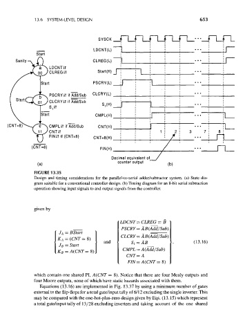
13.6  SYSTEM-LEVEL DESIGN                                            653


                                            SYSCK

                                          LDCNT(L)
                  Start
         Sanity^ /^                      CLREG(L)
                       LDCNTiT
                       CLREGiT             Start(H)J

                    Start                PSCRY(L)

                       PSCRYiT if Add/Sub  CLCRY(L)
                       CLCRYiT if Add/Sub
                       8,1?                  Sl(H)

                    Start                 CMPL(H)

                       CMPLit if Add/Sub    CNT(H)
                       CNTIT
                       FINitif(CNT=8)     CNT=8(H)

                (CNT=8)                     FIN(H)

                                                 Decimal equivalent of
                  / a\                              counter output  ~   /^

                 FIGURE 13.35
                 Design and timing considerations for the parallel-to-serial adder/subtractor system, (a) State dia-
                 gram suitable for a conventional controller design, (b) Timing diagram for an 8-bit serial subtraction
                 operation showing input signals to and output signals from the controller.


                 given by

                                                     LDCNT'= CLREG = B
                                                     PSCRY=AB(Add/Sub)
                           J A = BStart   }                   _ =
                           K =(CNT=8)                 CLCRY=AB(Add/Sub)
                                              and        S }=AB                    (13.16)
                           J B = Start
                                                      CMPL=A(Add/Sub)
                           K B = A(CNT = 8),
                                                       CNT=A
                                                        FIN=A(CNT=8)


                 which contain one shared PI, A(CNT = 8). Notice that there are four Mealy outputs and
                 four Moore outputs, none of which have static hazards associated with them.
                   Equations (13.16) are implemented in Fig. 13.37 by using a minimum number of gates
                 external to the flip-flops for a total gate/input tally of 6/12 excluding the single inverter. This
                 may be compared with the one-hot-plus-zero design given by Eqs. (13.15) which represent
                 a total gate/input tally of 13/28 excluding inverters and taking account of the one shared