Page 684 - Engineering Digital Design
P. 684

652              CHAPTER 13 / ALTERNATIVE SYNCHRONOUS FSM ARCHITECTURES


                                                                                                 0(H)
                      Sanity(L) -               FIN(H)
                 +V s  SYSCK —                  CMPL(H)                    P A  r P  r P  r D
                                                                                         P
                                                                           r
                                                                                B
                                                                                     C
                                                            LDCNT(L)    LD
                                                CLCRY(L)
          Start                                                              Parallel loadable  CL >0(L)
         Switch                                 PSCRY(L)    SYSCK            Up/Down Binary
                                 Controller
                                                                       CO       Counter     up
                                                CNT(H)
                                                                       BO                   Dn
                  Add/Sub(H)                » LDCNT(L)                                            CNT(H)
                                                             CNT = 8(H)
                    CNT = 8(H)              » CLREG(L)
                           "7 " 0" ''
                                        8
                                    p . . . p
                                    r     r
                                    A     H
                    SYSCK — )>        8-Bit     CL >- CLREG(L)
                                  Universal Shift
                       0(H)- R      Register     L -0(H)
                                                                      1
                               S  b Q  U O ' • » f~}
                                            U
                                1  O   A     H
                                                                      Cl
                                             I                    A _.
                    S^H)       '                                               — ^ Serialout(H)
                                                 CMPL(H) -^ ^^        FA  s
                                                                   B
                                                                     CO
                                1  0    A     H
                                                                                   SYSCK
                       0(H)- R        8-Bit      L -0(H)               L,
                            ,     Universal Shift
                        CK —  /     Register   CL 3- CLREG(L)      v   D
                                    p . . . p          CLCRY(L) — C CL   PR D  — PSCRY(L)
                                    r     r
                                    A     H
                                       \ 8                          Q    Q
                           B 7 -B 0 (H)  h                          V    1    1
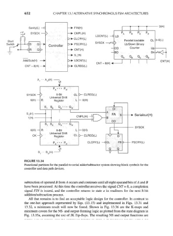
                    FIGURE 13.34
                    Functional partition for the parallel-to-serial adder/subtractor system showing block symbols for the
                    controller and data path devices.


                    subtraction of operand B from A occurs and continues until all eight operand bits of A and B
                    have been processed. At this time the controller receives the signal CNT= 8, a completion
                    signal FIN is issued, and the controller returns to state a in readiness for the next 8-bit
                    addition/subtraction process.
                      All that remains is to find an acceptable logic design for the controller. In contrast to
                    the one-hot approach represented by Eqs. (13.15) and implemented in Figs. 13.31 and
                    13.32, a minimum result will now be found. Shown in Fig. 13.36 are the K-maps and
                    minimum covers for the NS- and output-forming logic as plotted from the state diagram in
                    Fig. 13.35a, assuming the use of JK flip-flops. The resulting NS and output functions are
   679   680   681   682   683   684   685   686   687   688   689