
Page 679 - Engineering Digital Design
P. 679
13.5 THE ONE-HOT DESIGN METHOD 647
From the state diagram in Fig. 13.3la, the one-hot NS and output functions are read
directly by applying Eqs. (13.9), and the results are
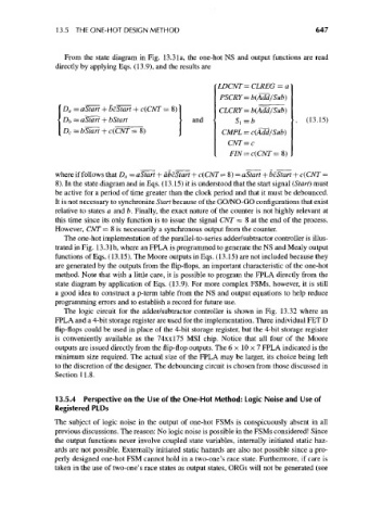
LDCNT'= CLREG = a
PSCRY=b(Add/Sub)
D a = aStart + bcStart + c(CNT - 8) CLCRY=b(Add/Sub)
D b = aStart + bStart and S\=b (13.15)
D c = bStart + c(CNT = 8) CMPL = c(Add/Sub)
CNT=c
FIN=c(CNT=8) \
where if follows that D a = aStart + abcStart + c(CNT= 8) = aStart + bcStart + c(CNT =
8). In the state diagram and in Eqs. (13.15) it is understood that the start signal (Start) must
be active for a period of time greater than the clock period and that it must be debounced.
It is not necessary to synchronize Start because of the GO/NO-GO configurations that exist
relative to states a and b. Finally, the exact nature of the counter is not highly relevant at
this time since its only function is to issue the signal CNT = 8 at the end of the process.
However, CNT = 8 is necessarily a synchronous output from the counter.
The one-hot implementation of the parallel-to-series adder/subtractor controller is illus-
trated in Fig. 13.31b, where an FPLA is programmed to generate the NS and Mealy output
functions of Eqs. (13.15). The Moore outputs in Eqs. (13.15) are not included because they
are generated by the outputs from the flip-flops, an important characteristic of the one-hot
method. Note that with a little care, it is possible to program the FPLA directly from the
state diagram by application of Eqs. (13.9). For more complex FSMs, however, it is still
a good idea to construct a p-term table from the NS and output equations to help reduce
programming errors and to establish a record for future use.
The logic circuit for the adder/subtractor controller is shown in Fig. 13.32 where an
FPLA and a 4-bit storage register are used for the implementation. Three individual FET D
flip-flops could be used in place of the 4-bit storage register, but the 4-bit storage register
is conveniently available as the 74xxl75 MSI chip. Notice that all four of the Moore
outputs are issued directly from the flip-flop outputs. The 6x10x7 FPLA indicated is the
minimum size required. The actual size of the FPLA may be larger, its choice being left
to the discretion of the designer. The debouncing circuit is chosen from those discussed in
Section 11.8.
13.5.4 Perspective on the Use of the One-Hot Method: Logic Noise and Use of
Registered PLDs
The subject of logic noise in the output of one-hot FSMs is conspicuously absent in all
previous discussions. The reason: No logic noise is possible in the FSMs considered! Since
the output functions never involve coupled state variables, internally initiated static haz-
ards are not possible. Externally initiated static hazards are also not possible since a pro-
perly designed one-hot FSM cannot hold in a two-one's race state. Furthermore, if care is
taken in the use of two-one's race states as output states, ORGs will not be generated (see