
Page 677 - Engineering Digital Design
P. 677
13.5 THE ONE-HOT DESIGN METHOD 645
Sanity(L) J~~ — |
Start(L) _l "H
Bin(H) I 1 j 1 1 •i 1 J
T(H) I 1 .._ 1 1 .J 1 J ™l
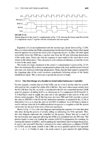
FIGURE 13.30
Timing diagram for the serial 2's complementer in Fig. 13.29, showing the binary input Bin and the
2's complement output T together with the initialization and start signals.
Equations (13.14) are implemented with the one-hot logic circuit shown in Fig. 13.29d.
Here, it is observed that the FSM is initialized into the 00 state following which a Start signal
must be applied over at least one clock cycle to begin the process. In effect, the Start signal
irreversibly forces the FSM into a one-hot state from the 00 state following deactivation
of the sanity input. Notice also that the sequence is open-ended in the sense that it never
returns to the initial state a. Thus, the process will continue ad infinitum, or until the circuit
is reset by the sanity input.
The results of a logic simulation of the serial 2's complementer is given in Fig. 13.30.
Here, the serial input Bin is shown synchronized in phase with clock, and the circuit is forced
into state a by Sanity(L) following initialization. Notice that the Start signal is sampled by
the triggering edge of the clock waveform immediately following release of the Sanity
initialization signal. This is necessary to permit the process to begin.
13.5.3 One-Hot Design of a Parallel-to-Serial Adder/Subtractor Controller
For this example, consider that two 8-bit USRs, one for word A and the other for word B,
shift each bit into a single Full Adder (FA) LSB first. The sum is then issued serially from
the FA LSB first. One bit, say bit B, is introduced to the FA via a controlled inverter (XOR
gate) for purposes of adding bit B to or subtracting (in 2's complement) bit B from bit A.
A D flip-flop is used to supply the carry-out of one operation to the carry-in of the next
bitwise serial operation. The D flip-flop must also have PRE and CLR overrides to preset
the carry-in (PSCRY) to the FA for the subtraction operation, as required by Eq. (2.14) in
Subsection 2.6.2, or to clear the carry-in (CLCRY) if addition. An n-bit binary counter is
used to indicate when the 8-bit addition/subtraction process is complete so that the system
can be reset for the next 8-bit series of bit-wise operations.
Shown in Fig. 13.3 la is the state diagram representing the sequence of events that must
take place during the process of serially adding or subtracting two 8-bit operands. Thus,
this state diagram represents the controller for the process. Notice that use is made of
the one-hot-plus-zero approach allowing the FSM to be initialized into the 000 state. The
process begins in state a by loading the counter (LDCNT) in preparation for counting, by
clearing the registers (CLREG), and by pushing the start button (Start) to begin the process.
In state b, the external D flip-flop is initialized for either subtraction or addition (PSCRY
or CLCRY), and the mode controls to the USRs are set to parallel load the 8-bit operands
(S\ = 1, SQ = 1). Finally, in state c the mode control Si goes inactive for right shifting