
Page 186 - System on Package_ Miniaturization of the Entire System
P. 186
Mixed-Signal (SOP) Design 161
used for integration since conductor losses (such as line profiles, surface roughness,
tolerance) and dielectric losses (such as loss tangent) degrade the Q of the inductors and
capacitors. Hence, high-frequency dielectric materials with low loss tangents, metals
with high conductivity, and processes that provide good surface finish and rectangular
line profiles are required. Since, the ICs are mounted on PCBs, a packaging technology
that is organic based is preferable since this can ultimately replace the PCB. Called
system-on-package (SOP), this enables the assembly of bare die ICs directly on the
integrated substrate containing embedded components in thin-film form.
In this chapter, LCP material has been used for integration. This material has a
relative permittivity of 2.95 and a loss tangent of 0.002, which are invariant from 1 to
100 GHz; a moisture absorption less than 0.04 percent; and a CTE that is matched to the
PCB [24]. The dielectric thickness is in the range of 1 to 8 mils. A parallel process can be
used with copper metallization, which results in rectangular line profiles with minimum
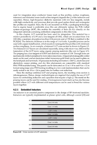
surface roughness. As an example, a balanced LCP cross section is shown in Figure 4.5.
Two balanced LCP layers are circuitized separately, along with micro-vias, followed by
lamination of the LCP layers using organic prepreg materials (the core in Figure 4.5).
The prepreg has a loss tangent of 0.0035 and dielectric constant of 3.38. Through holes are
mechanically drilled and plated to form interconnections. A liquid photoimageable solder
mask can be used, and an electroless nickel immersion gold finish can be used to plate on
the bond pads and terminals. All processes including lamination (<200°C), electroless and
electrolytic copper plating, and dry film photoresists are compatible with standard
FR4/PWB manufacturing. The panels can be fabricated on 12 in × 18 in and 9 in × 12 in
format using large-area PWB tooling resulting in a low-cost implementation that can be
easily scaled to an 18 in × 24 in panel size for further cost reduction.
Since the stackup combines LCP and prepreg layers, the resulting cross section is
inhomogeneous. Hence, design methodologies are required that enable the use of LCP
layers for embedding inductors and capacitors that require a high Q. The metal on the
prepreg layers can be used for routing. A homogeneous layer stack-up has also become
possible where LCP with different melt temperatures can be used to bond the various
layers together.
4.2.1 Embedded Inductors
An inductor is an essential passive component in the design of RF front-end modules.
Inductors are typically implemented as planar spiral coils, although coaxial [25] and
M1
Core 2–8 mils
M2
Core 1–4 mils
M3
LCP -1 mils
M4
Core 1–4 mils
M5
LCP -1 mils
M6
Core 1–4 mils
M7
Core 2–8 mils
M8
FIGURE 4.5 Cross section of LCP substrate.