
Page 188 - System on Package_ Miniaturization of the Entire System
P. 188
Mixed-Signal (SOP) Design 163
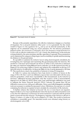
R sa
C s
L s R s
R 1 C 1 R 2 C 2
p
p
p
p
FIGURE 4.7 Equivalent circuit of inductor.
Because of the parasitic capacitance, the effective inductance changes as a function
of frequency. For a one-port inductor, either port 1 or 2 is grounded. For the circuit
model in Figure 4.7, the equations for L and Q can be derived analytically, or the
eff
response can be simulated using any circuit simulator. For the inductor parameters
defined earlier, the maximum Q attained is 36 in the frequency range between 4 to
5 GHz with an effective inductance of 2.7 nH. Clearly, the performance of the inductor
is being limited by the series resistance and the capacitance to ground. These parameters
can be minimized by using novel topologies (such as multilayer spirals) and maximizing
the distance to the ground plane.
It is possible to optimize the inductor layout using electromagnetic simulators, by
investigating new topologies and separating the ground plane from the inductor. The
results for a one-layer spiral inductor are shown in Table 4.2 [27]. Inductors A and B are
the same size inductors using different layers: inductor A is on the topmost layer M1 in
Figure 4.5 for achieving a higher Q factor, and inductor B is embedded on the top LCP
layer M3 which is 12 mils below. As shown in Table 4.2, the Q can be increased to 126 from
75. This result shows clearly the scalability of inductor Q using 3D integration.
In Table 4.2, various size inductors have been shown to achieve Q factors in the
range of 58 to 126. Sets 1 and 2 are different coupons that were fabricated with the same
inductor geometries, which show repeatability in the measurement. As the inductor Q
increases, calibration becomes important, since the accuracy of the Q measurements
depend on it. In Table 4.2, SOLT (short, open, load, and through) calibration was used
to calibrate the Vector Network Analyzer (VNA). Inductor Qs greater than 100 are
difficult to measure even with good calibration. Hence, good electromagnetic modeling
tools are necessary to confirm the measured values. Oftentimes, the response of a circuit
containing the inductor is required to back-calculate the unloaded Q of the inductor.
To further enhance the inductor Q beyond 126, two or more layers are required.
Figure 4.8 shows a two-layer spiral inductor where the layers are interconnected in such
a way that the inductance is enhanced, the series resistance is reduced, and the ground
plane is removed from the inductor. The frequency response of the inductor is shown in
Figure 4.9 where a Q value of 165 can be attained at 3.7 GHz. The model-to-hardware
correlation is reasonably good. The simulated results were obtained using Sonnet, an
electromagnetic solver [28].