
Page 187 - System on Package_ Miniaturization of the Entire System
P. 187
162 Cha pte r F o u r
Port 2
Width
Number of
turns
Spacing
Port 1
Ground plane
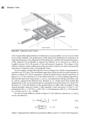
FIGURE 4.6 Single-layer spiral inductor.
wire-wound [26] implementations of inductors are also possible, on one or more metal
layers of the substrate. The performance of the inductor is dictated by its inductance at
a specified frequency, the unloaded Q at that frequency, and the self-resonant frequency
of the inductor. It is preferable to operate the inductor at its maximum Q, which is
roughly between 30 to 50 percent of the self-resonant frequency. The design of the
inductor requires careful optimization of the parasitics, which occur due to the parasitic
capacitance, conductor losses, and dielectric losses.
As an example, consider the inductor shown in Figure 4.6, which is implemented as
a spiral on an LCP layer. The broadband equivalent circuit for the two-port inductor is
shown in Figure 4.7, which represents a physical model of the inductor geometry. In
Figure 4.7, L is the inductance, R is the series resistance, C is the coupling capacitance
s s s
between the input and output ports, C and C are capacitors to the ground plane, and
p1
p2
R and R represent the dielectric loss. Resistor R is a fudge factor that enables the
sa
p2
p1
optimization of the circuit model based on simulated or measured data. For a fixed LCP
thickness of 1 mil and distance to the ground plane on either side of roughly 8 mils,
typical parasitic values for width = 1 mil, spacing = 1 mil, and turns = 1.5 are C = 2.7
s
femtofarads (fF), C = 33.7 fF, C = 492.1 fF, L = 2.5 nanohenries (nH), R = 1.39 ohms (Ω),
s
p2
p1
s
R = 6.6 kΩ, and R = R = 10 MΩ.
p2
p1
sa
For the two-port inductor model in Figure 4.7, the effective inductance L and Q
eff
can be calculated as:
⎛ 1 ⎞
L eff = Im ag ⎜ ⎝ 2π fY ⎠ ⎟ n = , 12 (4.1)
nn
Q = Imag Y ( nn ) n = ,12 (4.2)
Real Y ( )
nn
where Y represents the admittance parameters either at port 1 or 2 and f is the frequency.