
Page 185 - System on Package_ Miniaturization of the Entire System
P. 185
160 Cha pte r F o u r
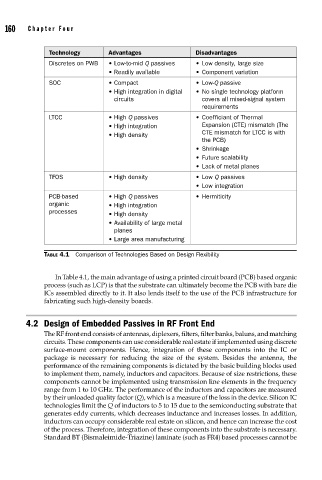
Technology Advantages Disadvantages
Discretes on PWB • Low-to-mid Q passives • Low density, large size
• Readily available • Component variation
SOC • Compact • Low-Q passive
• High integration in digital • No single technology platform
circuits covers all mixed-signal system
requirements
LTCC • High Q passives • Coefficiant of Thermal
• High integration Expansion (CTE) mismatch (The
• High density CTE mismatch for LTCC is with
the PCB)
• Shrinkage
• Future scalability
• Lack of metal planes
TFOS • High density • Low Q passives
• Low integration
PCB-based • High Q passives • Hermiticity
organic • High integration
processes
• High density
• Availability of large metal
planes
• Large area manufacturing
TABLE 4.1 Comparison of Technologies Based on Design Flexibility
In Table 4.1, the main advantage of using a printed circuit board (PCB) based organic
process (such as LCP) is that the substrate can ultimately become the PCB with bare die
ICs assembled directly to it. It also lends itself to the use of the PCB infrastructure for
fabricating such high-density boards.
4.2 Design of Embedded Passives in RF Front End
The RF front end consists of antennas, diplexers, filters, filter banks, baluns, and matching
circuits. These components can use considerable real estate if implemented using discrete
surface-mount components. Hence, integration of these components into the IC or
package is necessary for reducing the size of the system. Besides the antenna, the
performance of the remaining components is dictated by the basic building blocks used
to implement them, namely, inductors and capacitors. Because of size restrictions, these
components cannot be implemented using transmission line elements in the frequency
range from 1 to 10 GHz. The performance of the inductors and capacitors are measured
by their unloaded quality factor (Q), which is a measure of the loss in the device. Silicon IC
technologies limit the Q of inductors to 5 to 15 due to the semiconducting substrate that
generates eddy currents, which decreases inductance and increases losses. In addition,
inductors can occupy considerable real estate on silicon, and hence can increase the cost
of the process. Therefore, integration of these components into the substrate is necessary.
Standard BT (Bismaleimide-Triazine) laminate (such as FR4) based processes cannot be