
Page 195 - System on Package_ Miniaturization of the Entire System
P. 195
Mixed-Signal (SOP) Design 169
resonators that will resonate with the matching capacitors. Since the same set of passive
elements is used to simultaneously produce two passbands, this method translates to a
size and, hence, a cost-efficient solution for the future multiband, multifunctional
systems. The cross-coupling components between the input and output terminals provide
another transmission zero at the higher passband and thus control the bandwidth at the
higher frequency.
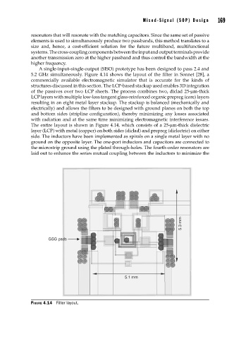
A single-input–single-output (SISO) prototype has been designed to pass 2.4 and
5.2 GHz simultaneously. Figure 4.14 shows the layout of the filter in Sonnet [28], a
commercially available electromagnetic simulator that is accurate for the kinds of
structures discussed in this section. The LCP-based stackup used enables 3D integration
of the passives over two LCP sheets. The process combines two, diclad 25-μm-thick
LCP layers with multiple low-loss tangent glass-reinforced organic prepreg (core) layers
resulting in an eight metal layer stackup. The stackup is balanced (mechanically and
electrically) and allows the filters to be designed with ground planes on both the top
and bottom sides (stripline configuration), thereby minimizing any losses associated
with radiation and at the same time minimizing electromagnetic interference issues.
The entire layout is shown in Figure 4.14, which consists of a 25-μm-thick dielectric
layer (LCP) with metal (copper) on both sides (diclad) and prepreg (dielectric) on either
side. The inductors have been implemented as spirals on a single metal layer with no
ground on the opposite layer. The one-port inductors and capacitors are connected to
the microstrip ground using the plated through-holes. The fourth-order resonators are
laid out to enhance the series mutual coupling between the inductors to minimize the
5.3 mm
GSG pads
5.1 mm
FIGURE 4.14 Filter layout.