
Page 200 - System on Package_ Miniaturization of the Entire System
P. 200
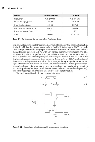
174    Cha pte r  F o u r


                      Device                     Commercial Balun            LCP Balun
                      Frequency                     4.8–5.9 GHz             4.8–5.9 GHz
                      Return loss (S ) (min)          16 dB                  −15.5 dB
                                 11
                      Insertion loss (max)            0.6 dB                 0.57 dB
                      Amplitude imbalance (max)       0.6 dB                 0.33 dB
                      Phase imbalance (max)             5°                      6°
                      Area                            9 mm 2                 5.16 mm 2

                    TABLE 4.4  Performance Comparisons of the Fabricated Balun

                    implementation compares to the commercially available balun with a 42 percent reduction
                    in size. In addition, the present balun can be embedded into the layers of LCP. Lumped-
                    element implementations using impedance matching networks have been proposed as a
                    means for size reduction [39]. As with any lumped-element approximation, this also
                    results in degradation in performance, particularly in amplitude imbalance across the
                    frequency bands. The lattice topology is a commonly used lumped-element solution for
                    implementing small-size narrow-band baluns, as shown in Figure 4.21. A combination of
                    low-pass and high-pass networks allows the splitting of the input signal into two output
                    signals that are equal in power but with a 180° phase difference. The low-pass and high-
                    pass networks can be implemented with as low a number as four passives (two inductors
                    and two capacitors), leading to small sizes (with the tradeoff of narrow-band operation).
                    The circuit topology also lends itself well to impedance transformation.
                       The design equations for the device are as follows:

                                               Z =  R source 1 ⋅  R load                 (4.7)
                                                0
                                                   Z          1
                                                L =  0   C =                             (4.8)
                                                   ω         Z ω
                                                     0        0  0

                                                         C
                                                                      Port 2
                                                               LL

                                      Port 1


                                                          L

                                                                      Port 3
                                                              C


                    FIGURE 4.21  Narrow-band balun topology with inductors and capacitors.