
Page 203 - System on Package_ Miniaturization of the Entire System
P. 203
Mixed-Signal (SOP) Design 177
0.02 pF Output 1
4.6 nH
144 nH
0.172 pF 0.172 pF
Input
7.39 nH 0.42 pF 7.39nH
4.6 nH
Output 2
0.92 pF
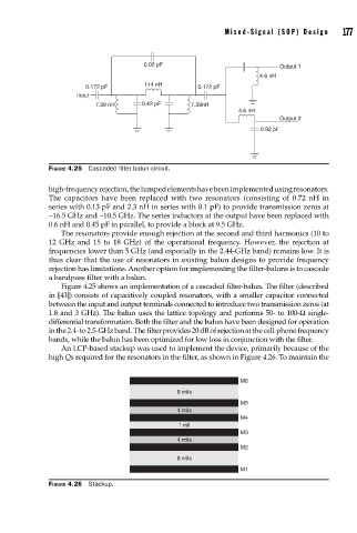
FIGURE 4.25 Cascaded fi lter balun circuit.
high-frequency rejection, the lumped elements have been implemented using resonators.
The capacitors have been replaced with two resonators (consisting of 0.72 nH in
series with 0.13 pF and 2.3 nH in series with 0.1 pF) to provide transmission zeros at
∼16.5 GHz and ∼10.5 GHz. The series inductors at the output have been replaced with
0.6 nH and 0.45 pF in parallel, to provide a block at 9.5 GHz.
The resonators provide enough rejection at the second and third harmonics (10 to
12 GHz and 15 to 18 GHz) of the operational frequency. However, the rejection at
frequencies lower than 5 GHz (and especially in the 2.44-GHz band) remains low. It is
thus clear that the use of resonators in existing balun designs to provide frequency
rejection has limitations. Another option for implementing the filter-baluns is to cascade
a bandpass filter with a balun.
Figure 4.25 shows an implementation of a cascaded filter-balun. The filter (described
in [43]) consists of capacitively coupled resonators, with a smaller capacitor connected
between the input and output terminals connected to introduce two transmission zeros (at
1.8 and 3 GHz). The balun uses the lattice topology and performs 50- to 100-Ω single-
differential transformation. Both the filter and the balun have been designed for operation
in the 2.4- to 2.5-GHz band. The filter provides 20 dB of rejection at the cell-phone frequency
bands, while the balun has been optimized for low loss in conjunction with the filter.
An LCP-based stackup was used to implement the device, primarily because of the
high Qs required for the resonators in the filter, as shown in Figure 4.26. To maintain the
M6
8 mils
M5
4 mils
M4
1 mil
M3
4 mils
M2
8 mils
M1
FIGURE 4.26 Stackup.