
Page 204 - System on Package_ Miniaturization of the Entire System
P. 204
178 Cha pte r F o u r
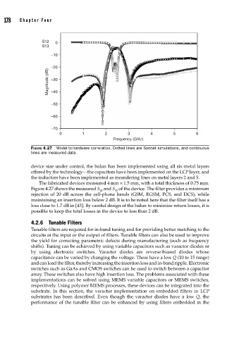
S12 0
S13
–10
–20
Magnitude (dB) –30
–40
–50
–60
–70
0 1 2 3 4 5 6
Frequency (GHz)
FIGURE 4.27 Model-to-hardware correlation. Dotted lines are Sonnet simulations, and continuous
lines are measured data.
device size under control, the balun has been implemented using all six-metal layers
offered by the technology—the capacitors have been implemented on the LCP layer, and
the inductors have been implemented as meandering lines on metal layers 2 and 5.
The fabricated devices measured 4 mm × 1.5 mm, with a total thickness of 0.75 mm.
Figure 4.27 shows the measured S and S of the device. The filter provides a minimum
21
31
rejection of 20 dB across the cell-phone bands (GSM, EGSM, PCS, and DCS), while
maintaining an insertion loss below 2 dB. It is to be noted here that the filter itself has a
loss close to 1.7 dB in [43]. By careful design of the balun to minimize return losses, it is
possible to keep the total losses in the device to less than 2 dB.
4.2.6 Tunable Filters
Tunable filters are required for in-band tuning and for providing better matching to the
circuits at the input or the output of filters. Tunable filters can also be used to improve
the yield for correcting parametric defects during manufacturing (such as frequency
shifts). Tuning can be achieved by using variable capacitors such as varactor diodes or
by using electronic switches. Varactor diodes are reverse-biased diodes whose
capacitance can be varied by changing the voltage. These have a low Q (10 to 15 range)
and can load the filter, thereby increasing the insertion loss and in-band ripple. Electronic
switches such as GaAs and CMOS switches can be used to switch between a capacitor
array. These switches also have high insertion loss. The problems associated with these
implementations can be solved using MEMS variable capacitors or MEMS switches,
respectively. Using polymer MEMS processes, these devices can be integrated into the
substrate. In this section, the varactor implementation on embedded filters in LCP
substrates has been described. Even though the varactor diodes have a low Q, the
performance of the tunable filter can be enhanced by using filters embedded in the