
Page 206 - System on Package_ Miniaturization of the Entire System
P. 206
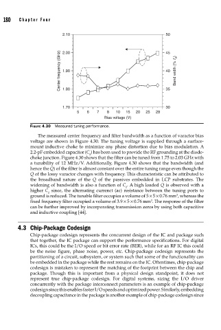
180    Cha pte r  F o u r


                                  2.10                                       50


                                 Center frequency (GHz)  1.90                40  Band width (% f a )
                                  2.00
                                                                             45


                                                                             35
                                  1.80


                                  1.70                                       30
                                        5   6   7   8   10  15  20   25  28
                                                   Bias voltage (V)
                    FIGURE 4.30  Measured tuning performance.
                       The measured center frequency and filter bandwidth as a function of varactor bias
                    voltage are shown in Figure 4.30. The tuning voltage is supplied through a surface-
                    mount inductive choke to minimize any phase distortion due to bias modulation. A
                    2.2-pF embedded capacitor (C ) has been used to provide the RF grounding at the diode-
                                             g
                    choke junction. Figure 4.30 shows that the filter can be tuned from 1.75 to 2.03 GHz with
                    a tunability of 12 MHz/V. Additionally, Figure 4.30 shows that the bandwidth (and
                    hence the Q) of the filter is almost constant over the entire tuning range even though the
                    Q of the lossy varactor changes with frequency. This characteristic can be attributed to
                    the broadband nature of the  Q of the passives embedded in LCP substrates. The
                    widening of bandwidth is also a function of C . A high loaded Q is observed with a
                                                            g
                    higher C  since, the alternating currenct (ac) resistance between the tuning ports to
                            g
                    ground is reduced. The tunable filter occupies a volume of 5 × 5 × 0.76 mm , whereas the
                                                                                 3
                                                                       3
                    fixed frequency filter occupied a volume of 3.9 × 5 × 0.76 mm . The response of the filter
                    can be further improved by incorporating transmission zeros by using both capacitive
                    and inductive coupling [44].
               4.3 Chip-Package Codesign
                    Chip-package codesign represents the concurrent design of the IC and package such
                    that together, the IC package can support the performance specifications. For digital
                    ICs, this could be the I/O speed or bit error rate (BER), while for an RF IC this could
                    be  the noise figure, phase noise, power, etc. Chip-package codesign represents the
                    partitioning of a circuit, subsystem, or system such that some of the functionality can
                    be embedded in the package while the rest remains on the IC. Oftentimes, chip-package
                    codesign is mistaken to represent the matching of the footprint between the chip and
                    package. Though this is important from a physical design standpoint, it does not
                    represent true chip-package codesign. For digital systems, sizing the I/O driver
                    concurrently with the package interconnect parameters is an example of chip-package
                    codesign since this enables faster I/O speeds and optimized power. Similarly, embedding
                    decoupling capacitance in the package is another example of chip-package codesign since