
Page 201 - System on Package_ Miniaturization of the Entire System
P. 201
Mixed-Signal (SOP) Design 175
= 3.48, tanδ = 0.004)
Rogers hydrocarbon (7.7 mils, ε r
= 10, tanδ = 0.019)
BC12TM (12 μm, ε r
Rogers hydrocarbon (7.7 mils, ε = 3.48, tanδ = 0.004)
r
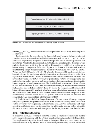
FIGURE 4.22 Stackup for balun implementation using high-K material.
where R source and R load are the source and load impedances, and w = 2πf is the frequency
0
0
of operation.
To demonstrate the operation of the lumped element balun, a balun operating at
2.44 GHz with a 100-MHz bandwidth has been designed. For an R source and R load of 50
and 100 Ω, respectively, this yields values of 0.92 pF and 4.6 nH for the capacitance and
inductance. With the thickness limitation restricting the use of multiple dielectric layers
and size limitations restricting the use of low-K materials, it is difficult to realize such
baluns using homogenous dielectrics. Figure 4.22 shows a 0.5-mm-thick stackup
incorporating a high dielectric constant material (Oak-Mitsui’s FaradFlex BC-12TM).
With a tan d of 0.019 and e = 10 (at 1 MHz) and a thickness of 12 μm, the material has
r
been developed for embedded digital decoupling applications. However, the high
capacitance density (11 nF/in at 1 MHz) makes this a suitable candidate for small size
2
low-profile baluns. The lattice topology is particularly suitable for design using this
material, as it uses low-pass and high-pass structures that are more tolerant to dielectric
losses compared to bandpass structures. The shielded device measures 1.25 mm × 2 mm
in area with a thickness of 0.507 mm, 1 dB of insertion loss, an amplitude imbalance of
2 dB, and a phase imbalance of ±10°. Table 4.4 shows the comparison of the fabricated
balun with a commercially available Marchand balun, also built on an organic substrate.
As can be seen from Table 4.3 the present balun implementation compares to the
commercially available balun with a 42 percent reduction in size. In addition, the
present balun can be embedded into the layers of LCP.
A third alternative in balun design is the use of transformers. Although compact
designs are possible, the performance of the balun in this case is very much dependent
on the coupling between primary and secondary coils. An SOP technology with high
coupling coefficients, achieved through tight metal-to-metal spacing or low dielectric
thickness or a combination of both, is required for the implementation of these baluns.
4.2.5 Filter-Balun Networks
In a receiver, the signal coming in from the antenna is single-ended in nature, but the
active circuitry (beginning with the LNA) is usually differential, as shown in Figure 4.23.
The single-ended signal is filtered using a bandpass filter and then converted to
differential mode using a balun. With SOP-based implementation, a circuit embedded