
Page 196 - System on Package_ Miniaturization of the Entire System
P. 196
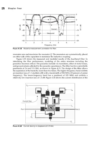
170    Cha pte r  F o u r


                               0                                                  5

                             –10                                                  0


                            S21, dB  –20                  Sonnet                  –5   S11, dB
                             –30
                                                                                  –10
                                                     Measured
                             –40                                                  –15

                             –50                                                  –20
                                1       2       3       4       5       6       7
                                                   Frequency, GHz
                    FIGURE 4.15  Model-to-measurement correlation for fi lter.

                    resonator area and maximize the resonator Q. The resonators are symmetrically placed
                    on either side of the capacitors to minimize the inductive coupling.
                       Figure 4.15 shows the measured and modeled results of the dual-band filter. In
                    simulating the filter performance, modeling of the entire structure including the
                    parasitics becomes critical. The parasitics include via transitions, effect of metal losses,
                    and ground returns affected by the parasitic capacitances. The filter has two controllable
                    passbands at 2.4 and 5.3 GHz, as shown in Figure 4.15. The design of the filter allows
                    the separation of the bands by more than two times. The higher-frequency band exhibits
                    an insertion loss of 1.1 decibels (dB) with a bandwidth of 530 MHz (10 percent of center
                    frequency). The lower-frequency band has a passband of 525 MHz and exhibits a
                    relatively low insertion loss of 1.3 dB. Figure 4.16 shows the current distribution of the


                                 C b

                                                                             L b


                                                                             L a
                              Current flow
                                                                             L c

                            Port 1                                               Port 2


                                     C c
                                                                            C f

                    FIGURE 4.16  Current density in stopband at 0.5 GHz.