
Page 205 - System on Package_ Miniaturization of the Entire System
P. 205
Mixed-Signal (SOP) Design 179
C ml C c C m2
L 1 C 1 L 2 C 2
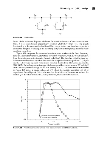
FIGURE 4.28 Tunable fi lter.
layers of the substrate. Figure 4.28 shows the circuit schematic of the varactor-tuned
filter. It is a second-order capacitively coupled Chebychev filter [44]. The circuit
functionality is the same as the dual-band filter except in this case the shunt capacitors
enable the designer to decouple the matching and passband frequency from the series
matching capacitors.
Figure 4.29 compares the measured results (square marker) of the fixed frequency
filter (i.e., instead of varactors, embedded capacitors were used) with the results obtained
from the electromagnetic simulator Sonnet (solid line). The data line with the × marker
is the measured result of a similar filter with the exception that the capacitors C (1.1 pF)
1
and C (1.1 pF) are replaced with silicon varactor diodes from Skyworks Inc. (model
2
SMV 1405). Each abrupt-junction-type diode can provide a capacitance of 2.7 to 0.6 pF
over a reverse junction voltage of 0 to 30 V (tuning of 4.2:1). The data of the tunable filter
in Figure 4.29 are at a tuning voltage of 6 V where the varactor provides 1.05 pF of
capacitance. From Figure 4.29 it can be seen that the addition of the varactor reduces the
loaded Q of the filter from 5.5 to 2.6 and, therefore, the bandwidth increases.
0
–5
S21, dB –10
–15
marker: Fixed frequency
marker: Tunable filter
–20
1.0 1.5 2.0 2.5 3.0
Frequency, GHz
FIGURE 4.29 Fixed-frequency and tunable fi lter measurements and EM simulations.