
Page 209 - System on Package_ Miniaturization of the Entire System
P. 209
Mixed-Signal (SOP) Design 183
where R is the source resistance, which is typically 50 Ω; b and g are bias-dependent
x
noise parameters of the MOSFET; and g is defined as the drain output conductance
do
evaluated at V = 0 V. In Equation (4.10), C is the correlation coefficient between the
ds
drain and gate noise currents of the FET.
Equation (4.10) shows that F is equally dependent on the parasitic resistances of
both gate and source inductors (R and R ). However, in practice, L is much smaller
g s s
than L and can be implemented as an on-chip or bond wire. However, depending on
g
the frequency of operation, L can be as high as 35 nH. The parasitic resistance of L (R )
g
g
g
is hence a very important contributor to the F of the LNA. As it is impossible to
implement this inductor on-chip, an optimum solution is to embed it in the package.
The Q of an inductor is a function of the signal loss within the device. The losses in an
inductor consist of two components, namely, losses in the metal and losses in the
dielectric. It has been shown that the inductor can be optimized for maximum Q. Under
these conditions, conductor losses dominate the total loss (and hence the Q). The
conductor losses can be reduced by increasing the conductor width (which reduces the
series resistance), leading to an increase in the size of the inductor, thus allowing for a
tradeoff of larger size for higher Q. By using embedded inductors in the package in
place of chip inductors for L , the designer has control over the required unloaded Q for
g
this inductor. However, because of the tradeoff with respect to size, using inductors
with the maximum Q possible is not a good strategy and could lead to unnecessarily
large sizes for the packaged LNA.
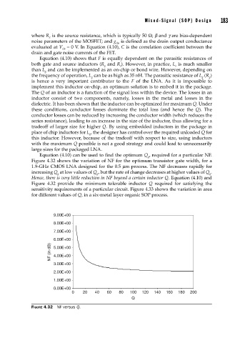
Equation (4.10) can be used to find the optimum Q , required for a particular NF.
g
Figure 4.32 shows the variation of NF for the optimum transistor gate width, for a
1.9-GHz CMOS LNA designed for the 0.5 μm process. The NF decreases rapidly for
increasing Q at low values of Q , but the rate of change decreases at higher values of Q .
g
g
g
Hence, there is very little reduction in NF beyond a certain inductor Q. Equation (4.10) and
Figure 4.32 provide the minimum tolerable inductor Q required for satisfying the
sensitivity requirements of a particular circuit. Figure 4.33 shows the variation in area
for different values of Q, in a six-metal layer organic SOP process.
9.00E+00
8.00E+00
7.00E+00
6.00E+00
NF (in dB) 5.00E+00
4.00E+00
3.00E+00
2.00E+00
1.00E+00
0.00E+00
0 20 40 60 80 100 120 140 160 180 200
Q
FIGURE 4.32 NF versus Q.