
Page 212 - System on Package_ Miniaturization of the Entire System
P. 212
186 Cha pte r F o u r
Chebyshev filter
f out1
f out2
Im(z) C i
Im(z)
Inductive L 1 C 1
L i
Capacitive
L 2 C 2
f (GHz) f v (GHz)
0.9 1.9
0.9 1.9
C 11 C c1 C 22
P o1
L a C s1 L a C s1
Chebyshev filter
C 33 C c2 C 44
P o2
C
L b s2 L b C s2
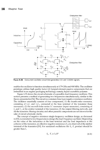
FIGURE 4.35 Concurrent oscillator circuit that generates 0.9- and 1.8-GHz signals.
enables the oscillator to function simultaneously at 1.79 GHz and 900 MHz. The oscillator
prototype utilizes high quality factor (Q) lumped-element passive components that are
embedded in an organic packaging technology, namely, liquid crystalline polymer.
Figure 4.35 shows the circuit schematic of a possible dual-frequency oscillator. This
section presents a method of generating two frequencies simultaneously, similar to the
theory presented in [54]. The circuit is a common-base type negative resistance oscillator.
The oscillator essentially consists of four components, (1) the fourth-order resonator,
consisting of L C and L C , connected at the base terminal of the transistor (base
1
1
2
2
resonator), (2) the second-order series LC resonator (input resonator), consisting of
L and C , at the emitter terminal of the transistor, (3) the output filtering network, and
i i
(4) the transistor. Biasing circuitry and other parasitic components are not shown for the
sake of circuit schematic clarity.
The concept of negative resistance single-frequency oscillator design, as discussed
in [53], is extended to two frequencies to design the dual-frequency oscillator. Depending
on the value of the inductance at the base terminal and the load impedance at the
collector of the transistor, an effective negative resistance (Z ) is observed at the emitter
in
terminal of the transistor [53]. For sustained oscillations the S ·Γ product should be
r
in
greater than 1,
S ⋅ Γ r ≥ ∠10 (4.11)
in