
Page 213 - System on Package_ Miniaturization of the Entire System
P. 213
Mixed-Signal (SOP) Design 187
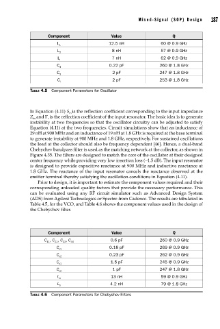
Component Value Q
L 1 12.5 nH 60 @ 0.9 GHz
L 8 nH 57 @ 0.9 GHz
2
L 7 nH 62 @ 0.9 GHz
i
C 1 0.22 pF 260 @ 1.8 GHz
C 2 2 pF 247 @ 1.8 GHz
C 2 pF 253 @ 1.8 GHz
i
TABLE 4.5 Component Parameters for Oscillator
In Equation (4.11) S is the reflection coefficient corresponding to the input impedance
in
Z and Γ is the reflection coefficient of the input resonator. The basic idea is to generate
in
r
instability at two frequencies so that the oscillator circuitry can be adjusted to satisfy
Equation (4.11) at the two frequencies. Circuit simulations show that an inductance of
29 nH at 900 MHz and an inductance of 19 nH at 1.8 GHz is required at the base terminal
to generate instability at 900 MHz and 1.8 GHz, respectively. For sustained oscillations
the load at the collector should also be frequency dependent [46]. Hence, a dual-band
Chebychev bandpass filter is used as the matching network at the collector, as shown in
Figure 4.35. The filters are designed to match the core of the oscillator at their designed
center frequency while providing very low insertion loss (∼1.5 dB). The input resonator
is designed to provide capacitive reactance at 900 MHz and inductive reactance at
1.8 GHz. The reactance of the input resonator cancels the reactance observed at the
emitter terminal thereby satisfying the oscillation conditions in Equation (4.11).
Prior to design, it is important to estimate the component values required and their
corresponding unloaded quality factors that provide the necessary performance. This
can be evaluated using any RF circuit simulator such as Advanced Design System
(ADS) from Agilent Technologies or Spectre from Cadence. The results are tabulated in
Table 4.5, for the VCO, and Table 4.6 shows the component values used in the design of
the Chebychev filter.
Component Value Q
C , C , C , C 44 0.6 pF 260 @ 0.9 GHz
33
22
11
C 0.18 pF 269 @ 0.9 GHz
c1
C 0.23 pF 262 @ 0.9 GHz
c2
C s1 1.5 pF 245 @ 0.9 GHz
C s2 1 pF 247 @ 1.8 GHz
L a 13 nH 59 @ 0.9 GHz
L 4.2 nH 79 @ 1.8 GHz
b
TABLE 4.6 Component Parameters for Chebyshev Filters