
Page 215 - System on Package_ Miniaturization of the Entire System
P. 215
Mixed-Signal (SOP) Design 189
as in Figure 4.37, detailed electromagnetic simulations become very time consuming
and hence circuit simulators become necessary.
The circuit is powered using two bench-top dc power supplies providing an emitter
voltage of –1.5 V and a collector supply of +1 V. Additional filtering of the power supply
noise is provided through microwave bias-tees and surface-mount decoupling capacitors.
The dual-frequency oscillator has been designed using a silicon bipolar transistor from
Agilent Technologies; a SOT-343 packaged bipolar transistor (HBFP 0420).
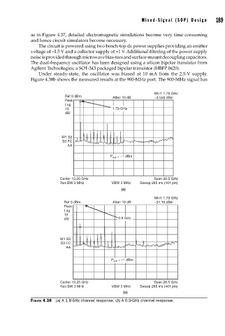
Under steady-state, the oscillator was biased at 10 mA from the 2.5-V supply.
Figure 4.38b shows the measured results at the 900-MHz port. The 900-MHz signal has
Mkr1 1.79 GHz
Ref 0 dBm
Atten 10 dB −3.558 dBm
Peak
Log
10 1.79 GHz
dB/
W1 S2
S3 FC
AA
P out = −1 dBm
Center 13.25 GHz Span 26.5 GHz
Res BW 3 MHz VBW 3 MHz Sweep 265 ms (401 pts)
(a)
Mkr1 1.79 GHz
Ref 0 dBm Atten 10 dB −31.15 dBm
Peak
Log
10
dB/ 0.9 GHz
W1 S2
S3 FC
AA
P out = +1 dBm
Center 13.25 GHz Span 26.5 GHz
Res BW 3 MHz VBW 3 MHz Sweep 265 ms (401 pts)
(b)
FIGURE 4.38 (a) A 1.8-GHz channel response. (b) A 0.9-GHz channel response.