Page 220 - System on Package_ Miniaturization of the Entire System
P. 220

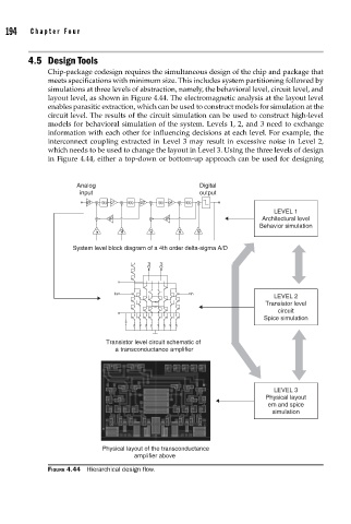
194    Cha pte r  F o u r


               4.5 Design Tools
                    Chip-package codesign requires the simultaneous design of the chip and package that
                    meets specifications with minimum size. This includes system partitioning followed by
                    simulations at three levels of abstraction, namely, the behavioral level, circuit level, and
                    layout level, as shown in Figure 4.44. The electromagnetic analysis at the layout level
                    enables parasitic extraction, which can be used to construct models for simulation at the
                    circuit level. The results of the circuit simulation can be used to construct high-level
                    models for behavioral simulation of the system. Levels 1, 2, and 3 need to exchange
                    information with each other for influencing decisions at each level. For example, the
                    interconnect coupling extracted in Level 3 may result in excessive noise in Level 2,
                    which needs to be used to change the layout in Level 3. Using the three levels of design
                    in Figure 4.44, either a top-down or bottom-up approach can be used for designing


                            Analog                          Digital
                             input                          output
                              g0  + I(s)  g1  +  I(s)  g3  +  I(s)  g4  +  I(s)  +
                                 -      -       -      -    -
                                                                                LEVEL 1
                                 +  g2         +   g5                        Architectural level
                                                                            Behavior simulation
                                 a1     a2      a3     a4   a5
                           System level block diagram of a 4th order delta-sigma A/D

                                               Out  Out


                                      In                  In
                                                                                LEVEL 2
                                                                             Transistor level
                                                                                 circuit
                                                                             Spice simulation


                                   Transistor level circuit schematic of
                                      a transconductance amplifier


                                                                                LEVEL 3
                                                                              Physical layout
                                                                              em and spice
                                                                               simulation


                                  Physical layout of the transconductance
                                           amplifier above
                    FIGURE 4.44  Hierarchical design fl ow.
   215   216   217   218   219   220   221   222   223   224   225