Page 224 - System on Package_ Miniaturization of the Entire System
P. 224

198    Cha pte r  F o u r


                    well as the width (ΔW) of the capacitors, illustrated in the previous numerical example,
                    is reverse-mapped from the component parameters as shown below

                                                          2
                                                3
                                     ΔL = 0.039(L ) + 0.982(L )  – 0.0674(L ) + 0.6104   (4.15)
                                                                   r
                                                         r
                                               r
                                                 3
                                                           2
                                     ΔS = 0.0231(C ) + 0.051(C )  – 0.0012(C ) + 0.032   (4.16)
                                                                     r
                                                r
                                                          r
                                                          2
                                                 3
                                    ΔW = –0.0009(k) + 0.351(k)  – 0.013(k) + 0.0123     (4.17)
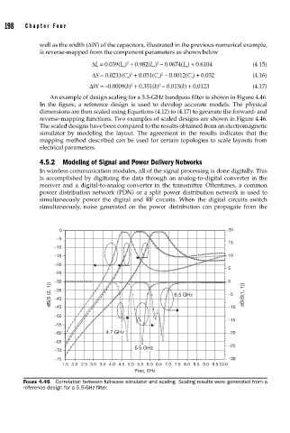
                       An example of design scaling for a 5.5-GHz bandpass filter is shown in Figure 4.46.
                    In the figure, a reference design is used to develop accurate models. The physical
                    dimensions are then scaled using Equations (4.12) to (4.17) to generate the forward- and
                    reverse-mapping functions. Two examples of scaled designs are shown in Figure 4.46.
                    The scaled designs have been compared to the results obtained from an electromagnetic
                    simulator by modeling the layout. The agreement in the results indicates that the
                    mapping method described can be used for certain topologies to scale layouts from
                    electrical parameters.
                    4.5.2  Modeling of Signal and Power Delivery Networks
                    In wireless communication modules, all of the signal processing is done digitally. This
                    is accomplished by digitizing the data through an analog-to-digital converter in the
                    receiver and a digital-to-analog converter in the transmitter. Oftentimes, a common
                    power distribution network (PDN) or a split power distribution network is used to
                    simultaneously power the digital and RF circuits. When the digital circuits switch
                    simultaneously, noise generated on the power distribution can propagate from the


                           0                                                    20
                          −5
                                                                                15
                         −10
                         −15                                                    10
                         −20
                                                                                5
                         −25
                         −30                                                    0
                        dB(S (2, 1))  −35                      6.5 GHz          −5   dB(S(1, 1))
                         −40
                         −45
                         −50                                                    −10
                                                                                −15
                         −55
                         −60             4.7 GHz                                −20
                         −65
                                                                                −25
                                                   5.5 GHz
                         −70
                         −75                                                    −30
                           1.5  2.0 2.5 3.0 3.5 4.0 4.5 5.0 5.5 6.0 6.5 7.0 7.5 8.0 8.5 9.0 9.5 10.0
                                                   Freq, GHz
               FIGURE 4.46  Correlation between full-wave simulator and scaling. Scaling results were generated from a
               reference design for a 5.5-GHz fi lter.
   219   220   221   222   223   224   225   226   227   228   229