
Page 223 - System on Package_ Miniaturization of the Entire System
P. 223
Mixed-Signal (SOP) Design 197
C_resn1 C_resn2
L_cp
Cc Cc
Lm
Lm
Lc Lc
L1 L2
Cp1 Cp1
Rc Rc
CC
Lr Cr Cr Lr
C Ls 2
Rs
R12 R12
Cp1 Cp2
C_m1
L1 L2
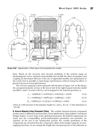
FIGURE 4.45 Segmentation of fi lter layout into lumped-element models.
them. Based on the two-port and one-port modeling of the sections using an
electromagnetic solver, lumped-circuit models that include the effect of parasitics and
coupling are developed. Because of the use of segmented models, fast optimization at
the circuit level is possible to meet design specifications without losing the effects of
physical layout on circuit performance.
The forward mapping is best explained with the help of Figure 4.45. In this figure,
the uncoupled inductor section in the lower half of the right lumped inductor model
(parallel L and C in series with R ) can be mapped to the inductor geometry as
r
r
12
2
3
L = –0.0024(ΔL) + 0.0273(ΔL) + 0.0674(ΔL) + 0.8104 (4.12)
r
3
2
C = –0.0009(ΔL) + 0.0051(ΔL) – 0.0009(ΔL) + 0.023 (4.13)
r
2
3
R = 0.0007(ΔL) + 0.111(ΔL) + 0.1082(ΔL) + 0.0942 (4.14)
12
where ΔL is the increase in the inductor length of L and L . For ΔL = 0, the inductance is
2
1
∼0.8 nH.
B. Reverse-Mapping Using Polynomial Fitting The scalable lumped-element component
models can be combined to perform filter circuit optimization using Agilent’s Advanced
Design System. At each stage of the optimization process, the desired components are
tuned and the corresponding polynomial-mapped geometries and parasitics are
updated. At the end of the optimization process, the variable geometries of the
components are extracted from the component values of the models using the reverse-
mapping functions. As an example the length (ΔL) and spacing (ΔS) of the inductors as