
Page 218 - System on Package_ Miniaturization of the Entire System
P. 218
192 Cha pte r F o u r
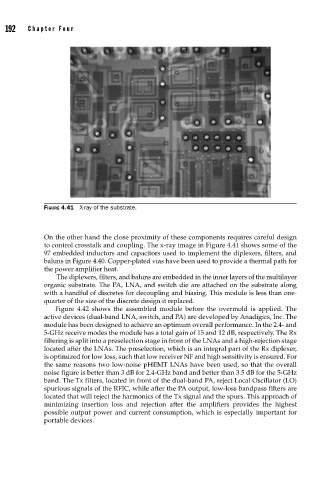
FIGURE 4.41 X-ray of the substrate.
On the other hand the close proximity of these components requires careful design
to control crosstalk and coupling. The x-ray image in Figure 4.41 shows some of the
97 embedded inductors and capacitors used to implement the diplexers, filters, and
baluns in Figure 4.40. Copper-plated vias have been used to provide a thermal path for
the power amplifier heat.
The diplexers, filters, and baluns are embedded in the inner layers of the multilayer
organic substrate. The PA, LNA, and switch die are attached on the substrate along
with a handful of discretes for decoupling and biasing. This module is less than one-
quarter of the size of the discrete design it replaced.
Figure 4.42 shows the assembled module before the overmold is applied. The
active devices (dual-band LNA, switch, and PA) are developed by Anadigics, Inc. The
module has been designed to achieve an optimum overall performance. In the 2.4- and
5-GHz receive modes the module has a total gain of 15 and 12 dB, respectively. The Rx
filtering is split into a preselection stage in front of the LNAs and a high-rejection stage
located after the LNAs. The preselection, which is an integral part of the Rx diplexer,
is optimized for low loss, such that low receiver NF and high sensitivity is ensured. For
the same reasons two low-noise pHEMT LNAs have been used, so that the overall
noise figure is better than 3 dB for 2.4-GHz band and better than 3.5 dB for the 5-GHz
band. The Tx filters, located in front of the dual-band PA, reject Local Oscillator (LO)
spurious signals of the RFIC, while after the PA output, low-loss bandpass filters are
located that will reject the harmonics of the Tx signal and the spurs. This approach of
minimizing insertion loss and rejection after the amplifiers provides the highest
possible output power and current consumption, which is especially important for
portable devices.