
Page 214 - System on Package_ Miniaturization of the Entire System
P. 214
188 Cha pte r F o u r
Micro-vias Thru-hole
Core2
M1–M2
Core1
M3–M4
LCP Core1
M5–M6
Core1
Core2
M7–M8
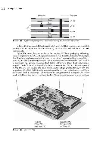
FIGURE 4.36 Eight-metal package cross section containing inductors and capacitors.
In Table 4.5, the unloaded Q values at the 0.9- and 1.8-GHz frequencies are provided,
which leads to the overall base resonator Q of 48 at 0.9 GHz and 36 at 1.8 GHz,
respectively.
Figure 4.36 shows the cross section of the multiple LCP layer packaging technology
used to implement the VCO. This process combines two diclad LCP layers with multiple,
low-loss tangent glass-reinforced organic prepreg (core) layers resulting in a multilayer
stackup. In total there are eight metal layers with the bottom-most metal layer used as
a microstrip-type ground reference. Each diclad LCP layer is 25 μm thick with ½ ounce
copper. The LCP dielectric layer has a dielectric constant of 2.95 and a loss tangent of
0.002. The low-loss tangent and thick metal results in high-Q inductors (Q > 100) and
capacitors (Q > 200). Additionally, microvias and buried vias with diameters <100 μm
have been used in the design. The layout of the design is shown in Figure 4.37, where
each metal layer is shown in a different color. With more components being embedded
Red: M1 Deep blue: M5
Yellow: M3 Dark green: M6
Light green: M4 Light blue: M8
FIGURE 4.37 Layout of VCO.