
Page 211 - System on Package_ Miniaturization of the Entire System
P. 211
Mixed-Signal (SOP) Design 185
Package Embedded inductor in
the package
3.5 mm
3.5 mm
(a)
15
S21 (dB)
10
NF (dB)
5
2.5 3
0
1 1.5 2
–5
–10
–15
S11, S22 (dB)
–20
–25
Frequency (GHz)
(b)
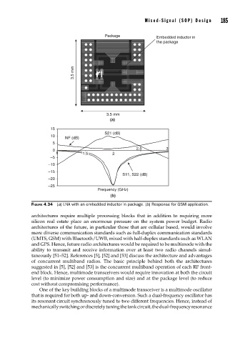
FIGURE 4.34 (a) LNA with an embedded inductor in package. (b) Response for GSM application.
architectures require multiple processing blocks that in addition to requiring more
silicon real estate place an enormous pressure on the system power budget. Radio
architectures of the future, in particular those that are cellular based, would involve
more diverse communication standards such as full-duplex communication standards
(UMTS, GSM) with Bluetooth/UWB, mixed with half-duplex standards such as WLAN
and GPS. Hence, future radio architectures would be required to be multimode with the
ability to transmit and receive information over at least two radio channels simul-
taneously [51–52]. References [5], [52] and [53] discuss the architecture and advantages
of concurrent multiband radios. The basic principle behind both the architectures
suggested in [5], [52] and [53] is the concurrent multiband operation of each RF front-
end block. Hence, multimode transceivers would require innovation at both the circuit
level (to minimize power consumption and size) and at the package level (to reduce
cost without compromising performance).
One of the key building blocks of a multimode transceiver is a multimode oscillator
that is required for both up- and down-conversion. Such a dual-frequency oscillator has
its resonant circuit synchronously tuned to two different frequencies. Hence, instead of
mechanically switching or discretely tuning the tank circuit, the dual-frequency resonance