
Page 210 - System on Package_ Miniaturization of the Entire System
P. 210
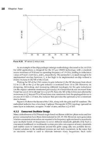
184    Cha pte r  F o u r


                             2.75

                                                                                  19


                            NF (in dB)                                                Area (in mm 2 )


                                                                                  16


                             2.25
                                     50   55   60    65   70    75   80    85   90
                                                        Q g
                    FIGURE 4.33  NF versus Q versus area.


                       As an example of the chip-package codesign methodology discussed so far, an LNA
                    for GSM applications is designed for the 0.5 μm CMOS technology, with a standard
                    source resistance of 50 Ω and an operating frequency of 1.9 GHz, leading to inductance
                    values of 9 and 1.2 nH for L  and L , respectively. The parameter L  is small enough to be
                                           g
                                                 s
                                                                          s
                    implemented on-chip; however, L  is too high to be implemented on-chip without a
                                                 g
                    drastic increase in the NF of the circuit.
                       Plotting the NF of the LNA versus its gate inductor Q, the NF decreases from about
                    5.2 to 2.1 dB as the Q of the gate inductor is increased from 10 to 200. However, on
                    designing, fabricating, and measuring different topologies for the gate inductance
                    (on the organic substrate mentioned previously), it is found that its size increased from
                         2
                                             2
                    9 mm  for a Q of 110 to 28 mm  for a Q of 170. Since the NF of the LNA is not affected by
                    an increase in Q  beyond 70 to 90 and since size constraints limit the packaged device to
                                 g
                    an area of 3.5 mm × 3.5 mm, the inductor that provides the optimum Q for a minimum
                    size is chosen.
                       Figure 4.34 shows the layout of the LNA, along with the gain and NF numbers. The
                    embedded inductor has a two-loop Coplanar Waveguide (CPW) topology (ground on
                                                      2
                    same layer as inductor), occupies ∼9 mm  of area, and has a Q of 110.
                    4.3.2  Concurrent Oscillator Design
                    Many embodiments of LCP-based single-band oscillators with low phase noise and low
                    power consumption have been demonstrated in [45, 49–50]. However, next-generation
                    wireless communication radios are required to be frequency agile and need to seamlessly
                    span multiple bands of frequencies to cover different standards globally [51]. Such a
                    concurrent multiband (or multimode) system provides convergence of many standards
                    and enables users to communicate around the globe using only one portable device.
                    Current solutions to the multiband systems are not truly concurrent, in the sense that
                    an electronic switch is used to alternate between many frequencies. Such radio