Page 208 - System on Package_ Miniaturization of the Entire System
P. 208

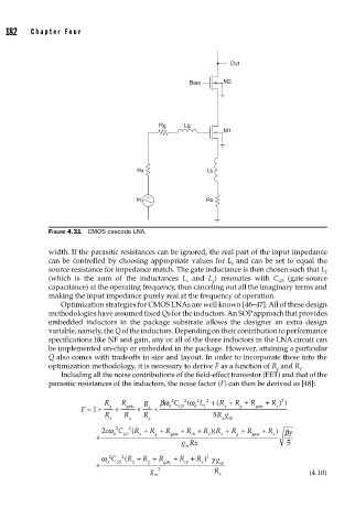
182    Cha pte r  F o u r


                                                                    Out


                                                         Bias     M2


                                                 Rg    Lg
                                                                  M1


                                           Rx                Ls


                                              +
                                           In                Rs


                    FIGURE 4.31  CMOS cascode LNA.

                    width. If the parasitic resistances can be ignored, the real part of the input impedance
                    can be controlled by choosing appropriate values for L  and can be set to equal the
                                                                    s
                    source resistance for impedance match. The gate inductance is then chosen such that L T
                    (which is the sum of the inductances  L  and  L ) resonates with  C  (gate-source
                                                                                GS
                                                               g
                                                        s
                    capacitance) at the operating frequency, thus canceling out all the imaginary terms and
                    making the input impedance purely real at the frequency of operation.
                       Optimization strategies for CMOS LNAs are well known [46–47]. All of these design
                    methodologies have assumed fixed Qs for the inductors. An SOP approach that provides
                    embedded inductors in the package substrate allows the designer an extra design
                    variable, namely, the Q of the inductors. Depending on their contribution to performance
                    specifications like NF and gain, any or all of the three inductors in the LNA circuit can
                    be implemented on-chip or embedded in the package. However, attaining a particular
                    Q also comes with tradeoffs in size and layout. In order to incorporate these into the
                    optimization methodology, it is necessary to derive F as a function of R  and R .
                                                                                      s
                                                                                g
                       Including all the noise contributions of the field-effect transistor (FET) and that of the
                    parasitic resistances of the inductors, the noise factor (F) can then be derived as [48]:
                                                                                 2
                                   R   R     R   βω  2 C  2  ω (  2 L  2  + ( R +  R +  R  +  R ))
                             F =+   g  +  gate  +  s  +  0  GS  0  T  x  g g  gate  s
                                1
                                   R    R    R                 5 Rg
                                    x    x    x                  x  do
                                   c 2 ω  2 C  2 ( R +  R +  R  + R +  R )( R + R +  R  +  R )  βγ
                                                        R
                                 +   0  GS  x   g   gate  ch  s  x   g   gate  s
                                                       gRx                        5
                                                        m
                                  ω  2 C  2 ( R + R +  R  +  R +  R ) γ g
                                                             2
                                             R
                                 +  0  GS  x  g   gate  ch  s    do
                                               g  2            R                        (4.10)
                                                m                x
   203   204   205   206   207   208   209   210   211   212   213