
Page 216 - System on Package_ Miniaturization of the Entire System
P. 216
190 Cha pte r F o u r
an output power of +1 dBm after de-embedding the 2-dB loss of the cable. It can be
observed that all the higher-order harmonics have been attenuated by more than 30 dB.
The 1.8-GHz signal has been measured simultaneously with the 900-MHz signal as
shown in Figure 4.38a. This signal has an output power of –1 dBm. At the 1.8-GHz port,
the 900-MHz signal is attenuated by at least 50 dB, as shown in Figure 4.38a. The phase
noise measurements are performed at only one port at a time to minimize the frequency
pulling of the oscillator during phase noise measurements. Both the signals measure a
phase noise of ∼–120 dBc/Hz at a 1-MHz offset. All the measurements here have been
made using a E4407B spectrum analyzer and a 8594E spectrum analyzer. Each of the
two second-order Chebychev filters have adjustable bandwidths and are designed to
provide a rejection of at least 30 dB at the other center frequency. Bandpass filters have
been used as matching networks to provide harmonic rejection (frequency domain) or
to provide a clean time-domain response. Thus the filters, in addition to harmonic
rejection, clean up the spectrum, which helps in obtaining a clean and accurate phase
noise measurement.
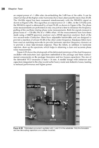
Figure 4.39 shows the photograph of the fabricated prototype of the dual-frequency
oscillator with inductors and capacitors embedded in the package and three surface-
mount components on the package (transistor and two bypass capacitors). The size of
the fabricated VCO measures 10 mm × 14 mm. A similar design with inductors and
capacitors integrated in the chip would suffer heavy metal and dielectric losses, leading
to reduced performance and higher power.
FIGURE 4.39 Fabricated concurrent oscillator with L and C in the substrate. Only the transistor
and two decoupling capacitors are surface mounted.