
Page 240 - System on Package_ Miniaturization of the Entire System
P. 240
214 Cha pte r F o u r
Estimated Actual
Layout Parameter Parameters Parameters
L1 m + 2.26s m + 2.29s
C_resn1/C_ren2 m − 1.66s m − 1.34s
CC m − 0.35s m − 0.71s
C_m1/C_m2 m + 2.27s m + 1.92s
TABLE 4.10 Probabilistic Diagnosis for Filter
4.6 Coupling
A mixed-signal system is subject to coupling between the digital and analog domains and
also within the analog domain. The modules or signals can couple from adjacent signal
routing lines, through the substrate, or electromagnetically between passive components.
This section discusses coupling and its undesirable effects on system or module
performance.
4.6.1 Analog-to-Analog Coupling
With higher levels of system integration, multiple passives embedded in the package
are necessary. An SOP-based receiver could then contain embedded passives for both
the LNA and VCO. As mentioned earlier, multiple embedded passives in the package
leads to system-level issues like feedback and resonance, many of which are not
apparent in an SOC implementation. To better understand these effects, circuits in the
2.1- and 2.4-GHz frequency bands are discussed, as described in this section.
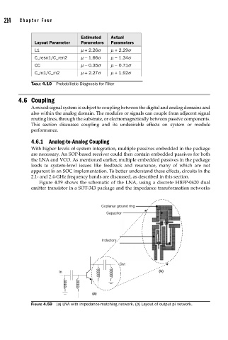
Figure 4.59 shows the schematic of the LNA, using a discrete HBFP-0420 dual
emitter transistor in a SOT-343 package and the impedance transformation networks
Coplanar ground ring
Capacitor
Inductors
Out
In (b)
(a)
FIGURE 4.59 (a) LNA with impedance-matching network. (b) Layout of output pi network.