
Page 242 - System on Package_ Miniaturization of the Entire System
P. 242
216 Cha pte r F o u r
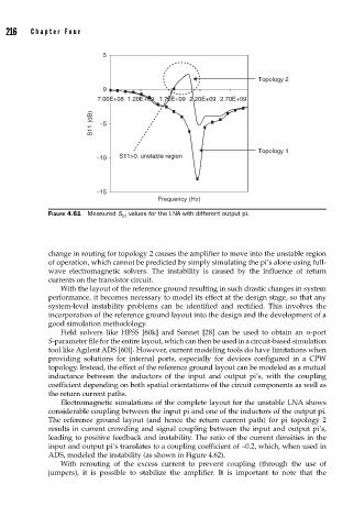
5
Topology 2
0
7.00E+08 1.20E+09 1.70E+09 2.20E+09 2.70E+09
S11 (dB) −5
Topology 1
−10 S11>0, unstable region
−15
Frequency (Hz)
FIGURE 4.61 Measured S 11 values for the LNA with different output pi.
change in routing for topology 2 causes the amplifier to move into the unstable region
of operation, which cannot be predicted by simply simulating the pi’s alone using full-
wave electromagnetic solvers. The instability is caused by the influence of return
currents on the transistor circuit.
With the layout of the reference ground resulting in such drastic changes in system
performance, it becomes necessary to model its effect at the design stage, so that any
system-level instability problems can be identified and rectified. This involves the
incorporation of the reference ground layout into the design and the development of a
good simulation methodology.
Field solvers like HFSS [60k] and Sonnet [28] can be used to obtain an n-port
S-parameter file for the entire layout, which can then be used in a circuit-based simulation
tool like Agilent ADS [60l]. However, current modeling tools do have limitations when
providing solutions for internal ports, especially for devices configured in a CPW
topology. Instead, the effect of the reference ground layout can be modeled as a mutual
inductance between the inductors of the input and output pi’s, with the coupling
coefficient depending on both spatial orientations of the circuit components as well as
the return current paths.
Electromagnetic simulations of the complete layout for the unstable LNA shows
considerable coupling between the input pi and one of the inductors of the output pi.
The reference ground layout (and hence the return current path) for pi topology 2
results in current crowding and signal coupling between the input and output pi’s,
leading to positive feedback and instability. The ratio of the current densities in the
input and output pi’s translates to a coupling coefficient of ∼0.2, which, when used in
ADS, modeled the instability (as shown in Figure 4.62).
With rerouting of the excess current to prevent coupling (through the use of
jumpers), it is possible to stabilize the amplifier. It is important to note that the