
Page 241 - System on Package_ Miniaturization of the Entire System
P. 241
Mixed-Signal (SOP) Design 215
implemented using high-Q embedded inductors and capacitors. The transistor is
biased in the common emitter configuration. The input and output of the transistor
are matched to 50 Ω by using LC pi networks, which are embedded in the package.
The output pi is designed for maximum power transfer and thus performs impedance
transformation from the complex conjugate of the collector impedance to 50 Ω.
The input pi is designed for a minimum noise figure and presents the Z to the gate
opt
of the transistor.
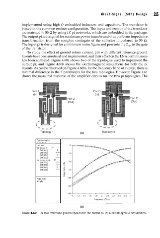
To study the effect of ground return current, pi’s with different reference ground
layouts have been modeled and implemented, and their effect on the LNA performances
has been analyzed. Figure 4.60a shows two of the topologies used to implement the
output pi, and Figure 4.60b shows the electromagnetic simulations for both the pi
layouts. As can be observed (in Figure 4.60b), for the frequency band of interest, there is
minimal difference in the S parameters for the two topologies. However, Figure 4.61
shows the measured response of the amplifier circuits for the two pi topologies. The
Port 1 Port 1
(In) (In)
Port 2 Port 2
(Out) (Out)
Topology 1 (a) Topology 2
Cartesian plot
ZO = 50.0
Left axis 0
for_sung_1
DB[S11]
DB[S12] −5
DB[S21]
DB[S22]
for_sung_jump
DB[S11] −10
DB[S12]
DB[S21]
DB[S22] Magnitude (dB) −15
−20
Right axis
[empty]
−25
−30
1 1.2 1.4 1.6 1.8 2 2.2 2.4 2.6 2.8 3
Frequency (GHz)
(b)
FIGURE 4.60 (a) Two reference ground layouts for the output pi. (b) Electromagnetic simulations.