
Page 245 - System on Package_ Miniaturization of the Entire System
P. 245
Mixed-Signal (SOP) Design 219
+ 2.7V
L b
C m
C 5
L c
C v
L 1 C 3
+ RF out
V tune
−
C 2 L 2 C 4
GND
FIGURE 4.64 Schematic of the TVCO [50].
undesired shift in the frequency of oscillation of the TVCO. A few possible scenarios
have been investigated based on the physical layout of the transformer as follows:
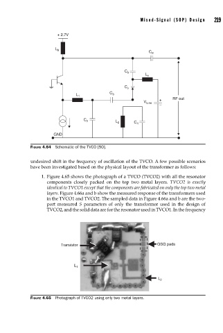
1. Figure 4.65 shows the photograph of a TVCO (TVCO2) with all the resonator
components closely packed on the top two metal layers. TVCO2 is exactly
identical to TVCO1 except that the components are fabricated on only the top two metal
layers. Figure 4.66a and b show the measured response of the transformers used
in the TVCO1 and TVCO2. The sampled data in Figure 4.66a and b are the two-
port measured S parameters of only the transformer used in the design of
TVCO2, and the solid data are for the resonator used in TVCO1. In the frequency
Transistor GSG pads
L 1
L 2
FIGURE 4.65 Photograph of TVCO2 using only two metal layers.