
Page 248 - System on Package_ Miniaturization of the Entire System
P. 248
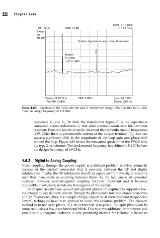
222    Cha pte r  F o u r


                                                                         Mkr1  5.10 GHz
                             Ref 0 dBm       Atten 10 dB                    –12.21 dBm
                             Samp
                             log           1
                             10 dB/
                                                    System alignments, align now, all required

                                                               2
                                             Marker
                                             5.1 GHz
                                             –12.21 dBm


                                 Center 13.25 GHz    VBH 3 MHz           Span 26.5 GHz
                                   Res BH 3 MHz                          Sweep 265 ms
                    FIGURE 4.69  Spectrum of the TVCO with the type 2 transformer design. The f 0  shifted to 5.1 GHz
                    from the design frequency of 1.9 GHz.


                           capacitors C  and  C . In both the transformer types,  C is the capacitance
                                      1      m                              1
                           connected across inductance  L  that adds a transmission zero for harmonic
                                                     1
                           rejection. From the results it can be observed that at nonharmonic frequencies
                           (4.95 GHz) there is considerable current at the output terminal (C ) that can
                                                                                    m
                           cause a significant shift in the magnitude of the loop gain and phase shift
                           around the loop. Figure 4.69 shows the measured spectrum of the TVCO with
                           the type 2 transformer. The fundamental frequency has shifted to 5.1 GHz from
                           the design frequency of 1.9 GHz.


                    4.6.2 Digital-to-Analog Coupling
                    Noise coupling through the power supply is a difficult problem to solve, primarily
                    because of the  physical connection that it provides between the RF and digital
                    subdomains. Ideally, the RF subdomain should be separated from the digital circuitry
                    such that there exists  no coupling between them.  As the frequencies of operation
                    increase, however, electromagnetic coupling becomes important and it becomes
                    impossible to completely isolate any two regions of the system.
                       As frequencies increase, power and ground planes are required to support a low-
                    inductance power delivery system. Though the planes have low-inductance properties
                    at high frequencies, they also couple energy, especially at their resonant frequencies.
                    Several techniques have been applied to solve this isolation problem. The classical
                    method is to use split planes. If a dc connection is required, the split planes can be
                    connected using a low-pass functional block. This requires additional components and
                    provides only marginal isolation. A very promising method for isolation is based on