Page 253 - System on Package_ Miniaturization of the Entire System
P. 253
Mixed-Signal (SOP) Design   227


                       The multiple plane structure in Figure 4.72 was fabricated using FR4 dielectric layers
                    with e = 4, tan d = 0.02, and thicknesses of 5 mils for each layer. Figure 4.74 shows that
                         r
                    there is excellent agreement regarding the transmission coefficient S  obtained from the
                                                                            12
                    measurement and simulations using a multilayered finite-difference method (FDM). S 12
                    is solely due to the coupling through the aperture and could be very accurately captured.
                    This is a large amount of coupling, which could cause a signal integrity problem if, for
                    example, the top and bottom planes were assigned to different voltage levels.


               4.7 Decoupling
                    The design of power distribution networks (PDN) is critical for the proper functionality
                    of a system. A major challenge in the design of the PDN is to maintain the impedance of
                    the network below the calculated target impedance over a broad frequency range. To
                    reduce the impedance, decoupling capacitors along with low-impedance interconnections
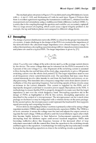
                    and planes are used in a typical PDN. The target impedance is given by [71]

                                                      V   × 5%
                                                   Z =  core                            (4.28)
                                                      I  × 50%
                                                       avg
                    where Vcore is the core voltage of the active device and Iavg is the average current drawn
                    by the device. The noise voltage that can be tolerated on the PDN is assumed to be
                    5 percent of the core voltage Vcore. Also 50 percent of the switching current is assumed
                    to flow during the rise and fall time of the clock edge, respectively, to give a 100 percent
                    switching current over the whole clock period [71]. The target impedance must be met
                    at all frequencies where current transients exist. The operations that may cause these
                    current transients involve data transfer to and from the hard disk and memory or on-
                    chip processing. This translates into a frequency range that varies from direct current to
                    multiples of the chip operating frequency. Fast switching speeds of these circuits cause
                    an increase in the current demands. This current is supplied by the PDN, and if
                    improperly designed could lead to excessive power supply fluctuations in the PDN. A
                    methodology to ensure thatthe PDN is properly designed is to make sure that the target
                    impedance is met over the whole frequency band. Decoupling capacitors aid in the
                    design of PDNs as highlighted in [72]. In this section, decoupling approaches are
                    described in the context of a microprocessor. The microprocessor can be a stand-alone
                    package on the board or may be integrated with a wireless device on the same package.
                    In the second option, the microprocessor could represent the baseband IC that supports
                    signal processing and computing functions.
                       Power delivery decoupling in today’s systems is primarilyachieved by using voltage
                    regulator modules (VRMs) and surface-mount discrete capacitors (SMDs). The VRM is a
                    dc-to-dc converter; it senses the voltage near the load and adjusts the output current to
                    regulate the load voltage. VRMs are effective until the lower kilohertz region after which
                    they become highly inductive in their behavior. Surface-mount capacitors provide
                    decoupling from the kilohertz region until several hundred megahertz. SMDs start
                    becoming ineffective above this frequency because of the increased effect of loop
                    inductance associated with the current flow from the capacitors to the switching circuits
                    and back again to the capacitors.A methodology for reducing the loop inductance would
                    be to place the decoupling capacitors as close to the switching circuits as possible.

