
Page 256 - System on Package_ Miniaturization of the Entire System
P. 256
230 Cha pte r F o u r
10 –1
Large
inductance
10 –2
Impedance (Ω)
10 –3
Target impedance
10 –4
10 2 10 3 10 4 10 5 10 6 10 7 10 8
Frequency (Hz) 100 MHz
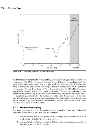
FIGURE 4.76 Decoupling limitations of SMD capacitors.
meet the target impedance of 0.78 mΩ for the 2007 processor using the above-mentioned
components. The SMDs are spread out on the board close to the package, with the
lower-value series inductance capacitors placed closer to the package. This has been
done to reduce the effect of the spreading inductance of the planes on the capacitor
performance. As seen from Figure 4.76, at frequencies close to 100 MHz it becomes
increasingly difficult to meet the target impedance. This can be attributed to the
increased effect of the loop inductance between the active circuits and the capacitors.
In order to provide effective decoupling above 100 MHz, it is essential to reduce the
effective inductance associated with the capacitors. One solution is to embed capacitors
within the package. Introduction of embedded capacitors reduces the current path
enabling decoupling above 100 MHz.
4.7.3 Embedded Decoupling
The focus of this section is on the performance of embedded capacitors. Embedded
capacitors can be broadly classified into two categories:
1. Planar capacitors. The power-ground plane in the package or the board is used
as a thin high-K (or low-K) capacitance layer.
2. Individual thick- or thin-film capacitors. Different-sized capacitors are used in a
layer of the package for decoupling.