
Page 251 - System on Package_ Miniaturization of the Entire System
P. 251
Mixed-Signal (SOP) Design 225
no need to consider multiple plane pairs. In reality, however, planes at the same dc level
have to be connected with vias to each other in order to reduce the effective inductance
of the planes. Such a via has to go through a via hole in a plane having a different dc
level, in order to avoid a short circuit. Through this via and via hole, fields in different
plane pairs get coupled to each other. As a result of this, there can be noise coupling not
only in the transversal direction between two planes, but also vertically from one plane
pair to another through the apertures and via holes. Coupling of multiple plane pairs
through such vias has been analyzed using the cavity resonator model [65], the
transmission matrix method [66], and coupled transmission lines [67].
In a multilayered stackup, the field penetration through the conductors can be neglected
for frequencies, where the skin depth is much smaller than the plane thickness. At lower
frequencies, this field penetration has to be taken into account [68]. Generally, skin effect is
pronounced above several megahertz for commonly used copper planes in packages.
In addition, planes generally have irregular geometries. There can be large apertures
and splits in planes. Fields in different plane pairs can get coupled through these
apertures. This can be regarded as a coupling by means of a wraparound current on the
edges of the planes. For narrow slots, a transmission-line based model has been
proposed to take into account this interlayer coupling [69]. Electric and magnetic
polarization currents have also been considered to compute coupling through electrically
small cutouts [70].
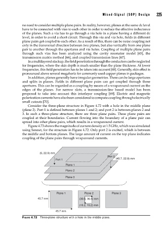
Consider the three-plane structure in Figure 4.72 with a hole in the middle plane
(plane 2). Port 1 is defined between planes 1 and 2; and port 2 is between planes 2 and
3. In such a three-plane structure, there are three plane pairs. These plane pairs are
coupled at their boundaries. Current flowing into the boundary of a plane pair can
spread into other plane pairs, which results in a wraparound current.
Figure 4.73 shows the magnitude of current density at 1.5 GHz, which was simulated
using Sonnet, for the structure in Figure 4.72. Only port 2 is excited, which is between
the middle and bottom planes. The large amount of current on the top plane indicates
coupling of the plane pairs through wraparound currents.
(0, 22.9) mm
Port 2
(45.7, 22.9) mm
Port 1
Plane 1
Plane 2
Plane 3
Plane 1 Plane 2 Plane 3
45.7 mm (30.5, 30.5) mm
(15.2, 15.2) mm
45.7 mm
FIGURE 4.72 Three-plane structure with a hole in the middle plane.