
Page 255 - System on Package_ Miniaturization of the Entire System
P. 255
Mixed-Signal (SOP) Design 229
Target
Feature size Impedance
Year (nm) Power (W) V (V) I (A) (m )
core avg
2004 90 84 1.2 70 1.7
2007 65 103.6 0.9 115.11 0.781
2010 45 119 0.6 198.33 0.302
TABLE 4.11 Target Impedance for Different Technology Nodes
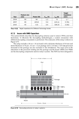
4.7.2 Issues with SMD Capacitors
This section briefly describes the decoupling schemes used in today’s PDNs and their
limitations. To illustrate the decoupling methodologies, a system simulation with
different decoupling components is performed. The schematic of the setup is shown in
Figure 4.75.
The setup includes a 10 cm × 10 cm board with a dielectric thickness of 0.8 mm and
metal thickness of 30 μm. A 4 cm × 4 cm package and a 11.8 mm × 11.8 mm processor
mounted on the package are also included in the simulations. The input port in the
simulation is the processor looking into the package and the board. SMDs and VRMs
are the decoupling components used in today’s system. The PDN has been designed to
4 cm × 4 cm
Port
P
G
Package
P
G
P
SMD’s
Power
V
R FR 4 0.8 mm
M
Ground
Board
10 cm × 10 cm
FIGURE 4.75 Decoupling schemes in today’s systems.