
Page 259 - System on Package_ Miniaturization of the Entire System
P. 259
Mixed-Signal (SOP) Design 233
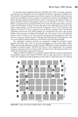
To meet the target impedance between 100 MHz and 2 GHz, a package capacitive
network has been designed with the embedded thick-film capacitors available from
DuPont [84]. An important requirement of these capacitors is to be able to place them as
close to the switching circuits as possible. The capacitive network can be designed with
all the discrete capacitors placed directly under or around the die shadow in the two
layers allocated to them in the package. The size of the die here is 11.8 mm × 11.8 mm
[85] for a cost performance processor for the 65-nm node. The placement of the capacitors
under the die shadow is done to reduce the effect of the spreading inductance of the
planes in the package. The network consists of eighteen 1 mm × 1 mm capacitors and
eighteen 0.75 mm × 0.75 mm capacitors in each discrete capacitor layer. The discrete
capacitors in the lower layer of the package are connected to the power and ground
bumps of the processor via blind and through vias. The layout of one of the discrete
layers is shown in Figure 4.79. The network is designed such that majority of the vias
from the capacitors connect directly to the flip-chip solder bumps of the processor. The
vias were modeled using FastHenry, an inductance extraction program [86].
The embedded capacitor network was designed to target the frequency band
between 100 MHz and 2 GHz. To provide decoupling over the entire band, VRMs,
SMDs, and on-chip capacitance are also required. SMDs and on-chip capacitance in this
example are effective below 100 MHz and above 2 GHz, respectively. The complete
frequency response is shown in Figure 4.80. The figure shows the frequency band over
which each decoupling component is effective.
VRMs are effective until the lower kilohertz region, SMDs provide decoupling from
the kilohertz region until around 100 MHz, and on-chip capacitance is used above
2 GHz. It is evident that target impedance on the order of 1 mΩ can be met over a broad
12 mm
Thru vias
12 mm
FIGURE 4.79 Layout of a discrete capacitor layer in the package.