
Page 263 - System on Package_ Miniaturization of the Entire System
P. 263
Mixed-Signal (SOP) Design 237
D3 = 0.120988 MM
D1 = 0.125 MM
D2 = 0.078125 MM
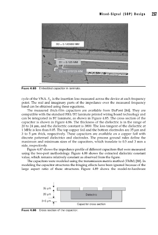
FIGURE 4.85 Embedded capacitor in laminate.
cycle of the VNA. S is the insertion loss measured across the device at each frequency
21
point. The real and imaginary parts of the impedance over the measured frequency
band can be obtained using these equations.
The measured thick-film capacitors are available from DuPont [84]. They are
compatible with the standard FR4/BT laminate printed wiring board technology and
can be integrated in BT laminate, as shown in Figure 4.85. The cross section of the
capacitor is shown in Figure 4.86. The thickness of the dielectric is in the range of
20 to 24 μm, and the dielectric constant is 3000. The loss tangent of the dielectric at
1 MHz is less than 0.05. The top copper foil and the bottom electrodes are 35 μm and
3 to 5 μm thick, respectively. These capacitors are available on a copper foil with
discrete patterned dielectrics and electrodes. The process ground rules define the
maximum and minimum sizes of the capacitors, which translate to 0.5 and 3 mm a
side, respectively.
Figure 4.87 shows the impedance profile of different capacitors that were measured
using the two-port methodology. Figure 4.88 shows the extracted dielectric constant
value, which remains relatively constant as observed from the figure.
The capacitors were modeled using the transmission matrix method (TMM) [88]. In
modeling the capacitor structures the fringing effects have been ignored because of the
large aspect ratio of these structures. Figure 4.89 shows the model-to-hardware
35 μm
20 μm Dielectric
3–5 μm
Capacitor cross section
FIGURE 4.86 Cross section of the capacitor.