
Page 262 - System on Package_ Miniaturization of the Entire System
P. 262
236 Cha pte r F o u r
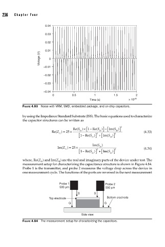
0.04
0.03
0.02
0.01
Vlotage (V) 0
–0.01
–0.02
–0.03
–0.04
0 0.5 1 1.5 2
Time (s) × 10 –8
FIGURE 4.83 Noise with VRM, SMD, embedded package, and on-chip capacitors.
by using the Impedance Standard Substrate (ISS). The basic equations used to characterize
the capacitor structures can be written as
)⎤ − ⎡
)⎤
Re(S ) × ⎡ ⎣ 1 − Re(S 21 ⎦ ⎣ Im(S 21 ⎦ ⎦ 2
Re(Z ) = 25 × 21 (4.33)
11 2 2
−
⎡1Re(S 21 ) ⎤ + ⎡Im(S 21 ⎤ ) ⎦
⎣
⎣
⎦
Im(S )
Im(Z ) = 25 × 21 (4.34)
11 2 2
⎡ ⎣ 1 − Re(S 21 ⎦ ⎣ Im(S 21 ⎦ ⎦
)⎤
)⎤ + ⎡
where, Re(Z ) and Im(Z ) are the real and imaginary parts of the device under test. The
11
11
measurement setup for characterizing the capacitance structure is shown in Figure 4.84.
Probe 1 is the transmitter, and probe 2 measures the voltage drop across the device in
one measurement cycle. The functions of the ports are reversed in the next measurement
Probe 1 Probe 2
500 μm 500 μm
S S
Top electrode Bottom electrode
G G
Side view
FIGURE 4.84 The measurement setup for characterizing the capacitors.