
Page 261 - System on Package_ Miniaturization of the Entire System
P. 261
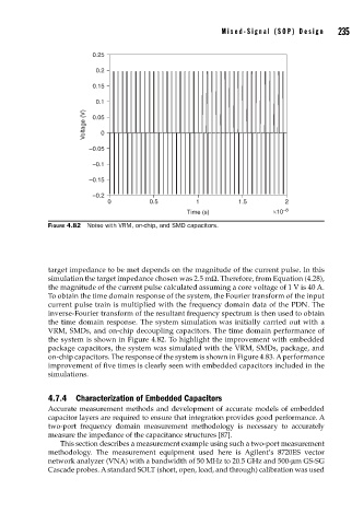
Mixed-Signal (SOP) Design   235


                                0.25

                                 0.2
                                0.15

                                 0.1
                              Voltage (V)  0.05


                                  0
                               –0.05

                                –0.1

                               –0.15
                                –0.2
                                    0          0.5         1          1.5         2
                                                         Time (s)              ×10 –8
                    FIGURE 4.82  Noise with VRM, on-chip, and SMD capacitors.


                    target impedance to be met depends on the magnitude of the current pulse. In this
                    simulation the target impedance chosen was 2.5 mΩ. Therefore, from Equation (4.28),
                    the magnitude of the current pulse calculated assuming a core voltage of 1 V is 40 A.
                    To obtain the time domain response of the system, the Fourier transform of the input
                    current pulse train is multiplied with the frequency domain data of the PDN. The
                    inverse-Fourier transform of the resultant frequency spectrum is then used to obtain
                    the time domain response. The system simulation was initially carried out with a
                    VRM, SMDs, and on-chip decoupling capacitors. The time domain performance of
                    the system is shown in Figure 4.82. To highlight the improvement with embedded
                    package capacitors, the system was simulated with the VRM, SMDs, package, and
                    on-chip capacitors. The response of the system is shown in Figure 4.83. A performance
                    improvement of five times is clearly seen with embedded capacitors included in the
                    simulations.


                    4.7.4  Characterization of Embedded Capacitors
                    Accurate measurement methods and development of accurate models of embedded
                    capacitor layers are required to ensure that integration provides good performance. A
                    two-port frequency domain measurement methodology is necessary to accurately
                    measure the impedance of the capacitance structures [87].
                       This section describes a measurement example using such a two-port measurement
                    methodology. The measurement equipment used here is  Agilent’s 8720ES vector
                    network analyzer (VNA) with a bandwidth of 50 MHz to 20.5 GHz and 500-μm GS-SG
                    Cascade probes. A standard SOLT (short, open, load, and through) calibration was used