
Page 30 - System on Package_ Miniaturization of the Entire System
P. 30
8 Cha pte r O n e
Building Blocks Traditional Technology SOP-based Technology
Package wiring Coarse wiring Ultrafine pitch, wiring in low-loss
Line width: 25 μm dielectrics
Pitch: 75 μm Line width: 2–5 μm
Pitch: 10–20 μm
Package-to-board Ball grid array (BGA) None!
interconnects bumps, tape automated
bonding (TAB)
Board wiring Very coarse-pitched wiring No PCB wiring. Package and PCB are
(line width/spacing: merged into the SOP substrate with
100–200 μm) ultrafine pitch wiring.
TABLE 1.1 (Continued)
1.4 System Technologies Evolution
The barriers to achieving the required miniaturization are circled in Figure 1.1. These are the
bulky IC packages, discrete components, connectors, cables, batteries, I/Os, massive thermal
structures, and the printed wiring boards on which all these are assembled. This approach to
system integration is called system-on-board (SOB). It constitutes 80 to 90 percent of traditional
electronic system size and more than 70 percent of the system manufacturing cost. In general,
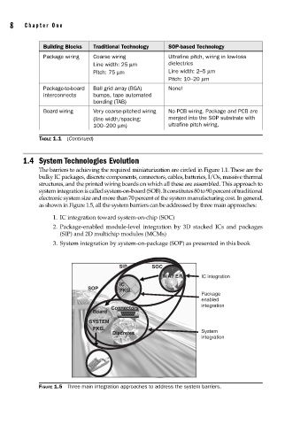
as shown in Figure 1.5, all the system barriers can be addressed by three main approaches:
1. IC integration toward system-on-chip (SOC)
2. Package-enabled module-level integration by 3D stacked ICs and packages
(SIP) and 2D multichip modules (MCMs)
3. System integration by system-on-package (SOP) as presented in this book
SIP SOC
WAFER IC integration
IC
SOP
PKG.
Package
enabled
integration
Connectors
Board
SYSTEM
PKG.
Discretes System
integration
FIGURE 1.5 Three main integration approaches to address the system barriers.