
Page 31 - System on Package_ Miniaturization of the Entire System
P. 31
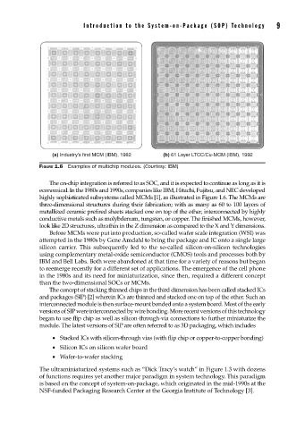
Intr oduction to the System-on-Package (SOP) Technology       9


                        (a) Industry’s first MCM (IBM), 1982  (b) 61 Layer LTCC/Cu-MCM (IBM), 1992

                    FIGURE 1.6  Examples of multichip modules. (Courtesy: IBM)

                       The on-chip integration is referred to as SOC, and it is expected to continue as long as it is
                    economical. In the 1980s and 1990s, companies like IBM, Hitachi, Fujitsu, and NEC developed
                    highly sophisticated subsystems called MCMs [1], as illustrated in Figure 1.6. The MCMs are
                    three-dimensional structures during their fabrication; with as many as 60 to 100 layers of
                    metallized ceramic prefired sheets stacked one on top of the other, interconnected by highly
                    conductive metals such as molybdenum, tungsten, or copper. The finished MCMs, however,
                    look like 2D structures, ultrathin in the Z dimension as compared to the X and Y dimensions.
                       Before MCMs were put into production, so-called wafer scale integration (WSI) was
                    attempted in the 1980s by Gene Amdahl to bring the package and IC onto a single large
                    silicon carrier. This subsequently led to the so-called silicon-on-silicon technologies
                    using complementary metal-oxide semiconductor (CMOS) tools and processes both by
                    IBM and Bell Labs. Both were abandoned at that time for a variety of reasons but began
                    to reemerge recently for a different set of applications. The emergence of the cell phone
                    in the 1980s and its need for miniaturization, since then, required a different concept
                    than the two-dimensional SOCs or MCMs.
                       The concept of stacking thinned chips in thethird dimension has been called stacked ICs
                    and packages (SIP) [2] wherein ICs are thinned and stacked one on top of the other. Such an
                    interconnected module is then surface-mount bonded onto a system board. Most of the early
                    versions of SIP were interconnected by wire bonding. More recent versions of this technology
                    began to use flip chip as well as silicon-through-via connections to further miniaturize the
                    module. The latest versions of SIP are often referred to as 3D packaging, which includes

                        •  Stacked ICs with silicon-through vias (with flip chip or copper-to-copper bonding)
                        •  Silicon ICs on silicon wafer board
                        •  Wafer-to-wafer stacking
                    The ultraminiaturized systems such as “Dick Tracy’s watch” in Figure 1.3 with dozens
                    of functions requires yet another major paradigm in system technology. This paradigm
                    is based on the concept of system-on-package, which originated in the mid-1990s at the
                    NSF-funded Packaging Research Center at the Georgia Institute of Technology [3].