
Page 53 - System on Package_ Miniaturization of the Entire System
P. 53
30 Cha pte r O n e
Digital block Analog block Optic block
Up-mixer
RF in
VCO Laser coiler
FPGA .... MUX D.S
Power combiner
Climer Amp
Multiple Class I-mixer
diffrential RF out Embedded optical detector
channel
VCO
FPGA .... DMUX S.D TIA Embedded
Power optical
doubler detector
(a)
3D Micro-channel network for
embedded active themal
management
Ultra-compact Ku-band
VCO Stacked microvias
cross-section view Embedded chip to
CPW inductor, 1 mm × 1 mm chip optoelectronics
High density wiring Embedded optical
Wire bond VCO die 25–50 μm lines/spaces Poly waveguides
waveguide
All other RF components 50–100 μm vias Polymer cross-section view
embedded in substrate waveguide
Digital ICs (μP) Buffer layer
RF IC (VCO)
Signal Signal
Inductors 30 μm
Signal 10 μm Ground
Filter Antenna Embedded C:10 nF/cm 2 , Power
10 μm film
Ground VCO ground
RF Digital section Optical
section Low CTE core substrate section
Stopped-impedance
low pass filter
Embedded RF
Inductors, VCO
filters, combiners
Embedded decoupling
Epoxy-BaTiO 3
Nanocomposite capacitor
Embedded 10–15 μm thin films, k~25 Cross-section of
antenna build-up layers
High density wiring
(b)
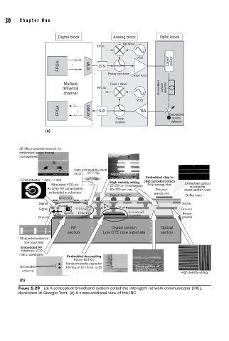
FIGURE 1.29 (a) A conceptual broadband system called the intelligent network communicator (INC),
developed at Georgia Tech. (b) A cross-sectional view of the INC.