
Page 50 - System on Package_ Miniaturization of the Entire System
P. 50
Intr oduction to the System-on-Package (SOP) Technology 27
MEMS Thermal WLP and assembly Integrated high density wiring-EIT,
Raytheon, TI, High heat flux-GE, HP, IBM, Lead free solders Asahi, IBM, Ibiden, Matsushita, Shipley,
University of SUN, Intel and Fujitsu Amkor, IBM, National Northrup Grumman, Hitachi, Samsung,
Arkansas Portable-Nokia, Sony, Semiconductor, Fujitsu, K&S, Materials-Promerus, Shipley, DuPont,
Motorola, Ericsson and Intel Unitive, Cookson DOW
Coating-SCS (Meniscus)
Curing-Lambda (Microwave)
Metallization-ATOTECH, Technics,
Shipley
Mixed
signal PD/TIA SOC MEMS Ga-As
test
IBM
Bromont Embedded opto
Agilent Back Plane-NTT, Siemens,
Infineon
Waveguides-Toray,
Reliability Kyocera, DuPont, Shipley,
Motorola DOW, GE
Intel MSM Detectors-Fraunhoffer,
IBM Kyocera
SONY BATTERY
TI
Signal and power integrity Embedded RF SOP
EMI-NEC Corp., Toshiba Embedded passives-IBM, EKC-DuPont, Sanmina, 3M,
Power distribution-Sun, Cadence, Intel, and AMD Boeing, Shipley, Motorola, Nokia, Intel, Amkar, Lucent, IMEC,
Signal integrity-IBM and Ansoft Kyocera
Embedded decoupling-Sanmina, EIT, DuPont Antennaes-Asahi, DoD, NASA
Design tools-Cadence, Sun, Motorola, HRL, Rambus Design tools-Cadence
FIGURE 1.25 R&D in SOP is now global.
Recently, IBM researchers have built an optical transceiver (Figure 1.27) in current
CMOS technology and coupled it with other optical components, made with materials
such as indium phosphide (InP) and GaAs, into a single integrated package only 3.25
by 5.25 mm in size. This compact design provides both a high number of communications
channels as well as very high speeds per channel. This transceiver chipset is designed
to enable low-cost optics by attaching to an optical board employing densely spaced
polymer waveguide channels using mass assembly processes. According to IBM, this
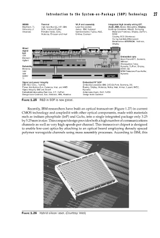
FIGURE 1.26 Hybrid silicon laser. (Courtesy: Intel)