
Page 45 - System on Package_ Miniaturization of the Entire System
P. 45
22 Cha pte r O n e
Optoelectronics, which today finds use primarily in the back plane and is used for
high-speed board interconnects, is expected to move onto the SOP package as chip-to-
chip high-speed interconnections replacing copper, thereby, addressing both the
resistance and crosstalk issues of electronic ICs. Optoelectronics, as it moves into silicon
as silicon photonics by Intel, is viewed, not as CMOS technology, but as an SOP-like
heterogeneous technology.
The SOP is about system integration enabled by thin-film integration of all system
components at microscale in the short term and nanoscale in the long term. As such, the
system package integration that SOP enables can be applied to CMOS ICs as overlays;
applied as thin films on top of silicon wafers (TFOS), silicon carriers, ceramic, and glass
substrates; or embedded into multilayer ceramics, packages, or board laminates.
1.6.1 Miniaturization Trend
The single most important parameter for digital convergence is system miniaturization.
It is now generally accepted that miniaturization leads to
• Higher performance
• Lower cost
• Higher reliability
• Higher functionality
• Smaller size
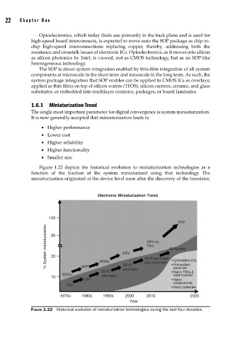
Figure 1.22 depicts the historical evolution to miniaturization technologies as a
function of the fraction of the system miniaturized using that technology. The
miniaturization originated at the device level soon after the discovery of the transistor,
Electronic Miniaturization Trend
100
SOP
% System miniaturization 80 SIPs 3D IC packages 3D System
SIPs by
TSV
20
MCMs
• Embedded
QFP
passives
packages
2D IC 3D IC and substrates • Embedded ICs
• Nano TIMs &
SOCs heat transfer
10 packages
CSP • Nano
components
ICs
• Nano batteries
1970s 1980s 1990s 2000 2010 2020
Year
FIGURE 1.22 Historical evolution of miniaturization technologies during the last four decades.