
Page 41 - System on Package_ Miniaturization of the Entire System
P. 41
18 Cha pte r O n e
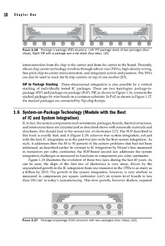
FIGURE 1.16 Package-in-package (PiP) structure. Left: PiP package stack of two packages (four
chips). Right: PiP with a package and a die stack (four dies). [16]
interconnection from the chip to the carrier and from the carrier to the board. Presently,
silicon chip carrier technology involves through-silicon vias (TSVs), high-density wiring,
fine pitch chip-to-carrier interconnection, and integrated actives and passives. The TSVs
can also be used to stack the Si chip carriers on top of one another [15].
SIP by Package Stacking Three-dimensional integration is also possible by a vertical
stacking of individually tested IC packages. There are two topologies: package-in-
package (PiP) and package-on-package (PoP). PiP, as shown in Figure 1.16, connects the
stacked packages by wire bonds on a common substrate. In PoP, as shown in Figure 1.17,
the stacked packages are connected by flip-chip bumps.
1.6 System-on-Package Technology (Module with the Best
of IC and System Integration)
If, in fact, the system components such as batteries, packages, boards, thermal structures,
and interconnections are miniaturized as described above with nanoscale materials and
structures, this should lead to the second law of electronics [17]. The SOP described in
this book is exactly that, and it (Figure 1.18) achieves true system integration, not just
with the best IC integration as in the past but also with the best system integration. As
such, it addresses then the 80 to 90 percent of the system problems that had not been
addressed, as described earlier. In contrast to IC integration by Moore’s law, measured
in transistors per cubic centimeter, the SOP-based second law addresses the system
integration challenges as measured in functions or components per cubic centimeter.
Figure 1.18 illustrates the evolution of these two laws during the last 40 years. As
can be seen, the slope of the first law of electronics is very steep, driven by the
unparalleled growth in the IC integration from one transistor in the 1950s to as many as
a billion by 2010. The growth in the system integration, however, is very shallow as
2
measured in components per square centimeter (cm ) on system-level boards to less
2
than 100/cm in today’s manufacturing. This slow growth, however shallow, required
FIGURE 1.17 Package-on-package (PoP) structure with two packages (four chips). [16]