
Page 39 - System on Package_ Miniaturization of the Entire System
P. 39
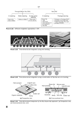
SIP


                         Through-Silicon Via (TSV)                   Non-TSV

                  IC stacking  Wafer stacking  Si chip carrier  IC stacking  Package stacking
                                             stacking
                 - Die-to-Die  - Wafter-to-Wafer  - Chip carrier-  Die-to-Die  - Package-on-Package (PoP)
                 - Die-to-Wafer           to-Chip carrier  - TAB        - Package-in-Package (PiP)
                                                          - Wire bond   - Folded stackable chip scale
                                                          - Side metallization    package (FSCSP)
                                                          - Embedded IC
                                                          - Flip chip
               FIGURE 1.11  Different integration approaches in SIP.


                    FIGURE 1.12  Three-dimensional integration using wire bonding.


                    FIGURE 1.13  Three-dimensional integration using a combination of fl ip-chip and wire bonding.


                       Heat spreader    Underfill resin
                                                                  Base-chip  Silicone resin
                                            Base-chip
                                                          Heat spreader           Underfill resin


                                               Solder ball
                      Organic substrate                      Substrate  Bump  Sub-chip  Solder ball
                                           Bump
                                (a) Perspective view              (b) Cross-sectional view
                    FIGURE 1.14  Three-dimensional integration by the fl ip chip-on-chip approach. (a) Perspective view.
                    (b) Cross-sectional view. [13]

               16