
Page 40 - System on Package_ Miniaturization of the Entire System
P. 40
Intr oduction to the System-on-Package (SOP) Technology 17
miniaturization and flexibility for the adaptation to different applications can be
achieved by using the 3D integration technologies. It also enables the combination of
different optimized technologies with the potential of low-cost fabrication through high
yield, smaller footprints, and multifunctionality. Three-dimensional technologies also
reduce the wiring lengths for interchip and intrachip communication. It thus provides
a possible solution to the increasingly critical “wiring crisis” caused by signal
propagation delays at both the board and the chip level.
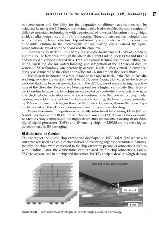
It is possible to stack multiple bare dies using die-to-die vias and TSVs as shown in
Figure 1.15. The latter run through the silicon die [Front End of Line (FEOL) and BEOL]
and are used to connect stacked dies. There are various technologies for via drilling, via
lining, via filling, die (or wafer) bonding, and integration of the 3D stacked dies (or
wafers). TSV technology can potentially achieve much higher vertical interconnect
density as compared to the other approaches for 3D integration discussed above.
The dies can be bonded in a face-to-face or in a face-to-back. In the face-to-face die
stacking, two dies are stacked with their BEOL areas facing each other. In the face-to-
back die stacking, two dies are stacked with the BEOL areas of one die facing the active
area of the other die. Face-to-face bonding enables a higher via density than face-to-
back bonding because the two chips are connected by die-to-die vias which have sizes
and electrical characteristics similar to conventional vias that connect on chip metal
routing layers. On the other hand, in face-to-back bonding, the two chips are connected
by TSVs which are much bigger than the BEOL vias. However, if more than two chips
are to be stacked, then TSVs are necessary even for face-to-face bonding.
Three-dimensional integration was initially introduced by stacking Flash (NOR/
NAND) memory and SDRAM for cell phones in one thin CSP. This was later extended
to Memory/Logic integration for high performance processors. Stacking of an ASIC
digital signal processors (DSPs) and RF/analog chips or MEMS are the next logical
developments in 3D packaging.
Si Substrate or Carrier
The concept of the silicon chip carrier was developed in 1972 [14] at IBM where a Si
substrate was used as a chip carrier instead of insulating organic or ceramic substrates.
Initially, the chips were connected to the chip carrier by perimeter connections such as
wire bonding. Later, the connections were replaced by flip-chip connections. Lately,
TSVs have been used in the chip and the carrier. The TSVs help to develop a high-density
Stacked Si devices (4-layered)
50 μm × 4
Interposer (Si) 1 mm
FIGURE 1.15 Three-dimensional integration with through-silicon-via technology.